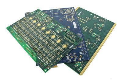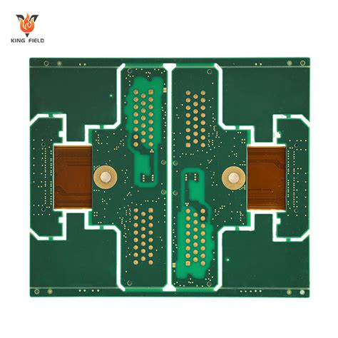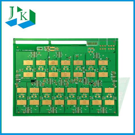
Rigid flex pcb stackup
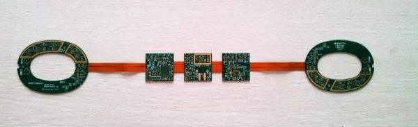
A rigid-flex PCB stackup is a combination of rigid and flexible PCBs that are interconnected to form a single board.
The stackup typically consists of several layers of rigid and flexible materials that are laminated together to create a single board.
The layers are arranged in a specific order to provide the required mechanical and electrical properties.

The typical stackup for a rigid-flex PCB consists of the following layers:
1. Coverlay:
This layer is a flexible material that covers the entire board, providing protection and insulation.
2. Flexible circuit:
This layer is made of a flexible material such as polyimide or polyester, and contains the conductive traces and vias.
3. Adhesive:
This layer is used to bond the flexible circuit to the rigid layers.
4. Rigid layer:
This layer is made of a rigid material such as FR4 or polyimide, and provides mechanical support and stability to the board.
5. Copper layer:
This layer contains the copper traces and pads that connect the components on the board.
6. Prepreg:
This layer is a resin-impregnated fiberglass material that is used to bond the copper layer to the rigid layer.
7. Rigid layer:
This layer provides additional mechanical support and stability to the board.
8. Copper layer:
This layer contains the copper traces and pads that connect the components on the board.
9. Prepreg:
This layer is used to bond the copper layer to the coverlay.
10. Coverlay: This layer provides protection and insulation to the board.
The exact stackup configuration may vary depending on the specific requirements of the application.

the role of rigid flex pcb stackup
The role of rigid-flex PCB stackup is to provide a combination of rigid and flexible circuitry in a single board.
This allows for greater design flexibility and reduces the need for multiple boards and connectors.
The stackup includes multiple layers of rigid and flexible materials that are bonded together to create a single board.
The rigid layers provide support and stability for components while the flexible layers allow for bending and folding of the board.
The stackup also includes vias and other interconnects to allow for communication between the rigid and flexible sections of the board.
The proper design and implementation of the rigid-flex PCB stackup is critical to ensure reliable and efficient operation of the board.

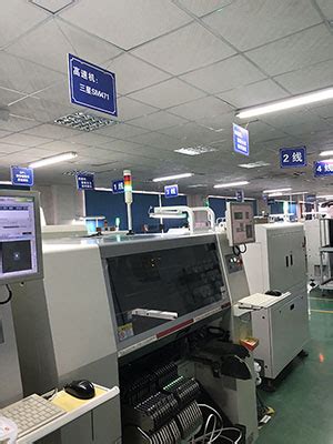
rigid flex pcb manufacturing process
The manufacturing process for rigid flex PCBs typically involves the following steps:
1. Design and layout:
The first step is to design the rigid flex PCB and create a layout that meets the requirements of the application.
This involves determining the size and shape of the board, the placement of components, and the routing of traces.
2. Material selection:
The next step is to select the materials that will be used to construct the rigid flex PCB.
This includes choosing the substrate material for the rigid sections and the flexible material for the flex sections.
3. Cutting and drilling:
Once the materials have been selected, the rigid and flexible sections are cut to size and drilled to accommodate the components and traces.
4. Layer bonding:
The layers of the rigid and flexible sections are bonded together using a combination of heat, pressure, and adhesive.
5. Plating and etching:
The next step is to apply a layer of copper to the surface of the board and then etch away the excess copper to create the desired traces and pads.
6. Component placement:
The components are then placed onto the board and soldered in place.
7. Testing and inspection:
The finished board is tested and inspected to ensure that it meets the required specifications and quality standards.
8. Final assembly:
Finally, the rigid flex PCB is assembled into the final product, which may include additional components, enclosures, and other features.