Seed Fusion PCB: Innovating the Future of Electronic Manufacturing
Introduction
Printed circuit boards (PCBs) play a vital role in the design and manufacturing of modern electronic devices. With the continuous advancement of science and technology, traditional PCB manufacturing methods are gradually unable to meet the growing market demand and technical requirements. As an emerging manufacturing technology, Seed Fusion PCB is changing the landscape of the electronics manufacturing industry with its high efficiency, flexibility and environmental protection. This article will explore the concept, advantages, applications and future development trends of Seed Fusion PCB in depth.
What is Seed Fusion PCB?
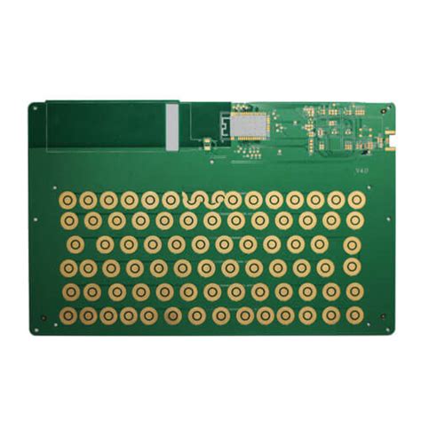
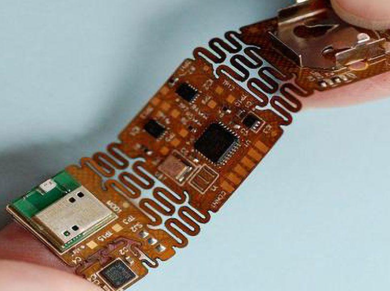
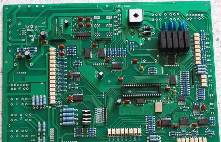
Seed Fusion PCB is a new type of printed circuit board based on advanced materials and manufacturing technology. It combines the advantages of traditional PCB manufacturing process with modern 3D printing technology, using high-performance conductive materials and polymers to form complex circuit structures through precise printing and fusion processes. This technology not only improves the production efficiency of PCBs, but also reduces production costs, and is particularly suitable for small-batch and diversified electronic product manufacturing.
How Seed Fusion PCB works
The manufacturing process of Seed Fusion PCB mainly includes the following steps:
Design stage: Use computer-aided design (CAD) software for circuit design and generate 3D models.
Material selection: Choose suitable conductive materials and substrates, usually using highly conductive metal powders and polymer substrates.
3D printing: Using 3D printing technology, the conductive material is printed layer by layer onto the substrate to form a circuit pattern.
Heat treatment: Through the heat treatment process, the conductive material is firmly bonded to the substrate to ensure the stability and conductivity of the circuit.
Post-processing: The finished product is cleaned, tested and packaged to ensure that it meets quality standards.

Advantages of Seed Fusion PCB
1.Efficiency
The manufacturing process of Seed Fusion PCB is more efficient than traditional PCB manufacturing processes. Due to the use of 3D printing technology, rapid prototyping can be achieved, shortening the product design to production cycle. This is especially important for electronic products that require frequent iterations and fast time to market.
2.Flexibility
Seed Fusion PCB can easily cope with small-batch and diversified production needs. Traditional PCB manufacturing usually requires large-scale production to reduce costs, while Seed Fusion PCB can maintain low costs and high quality in small-batch production. This enables companies to quickly adjust production plans according to market demand.
3.Environmental protection
Today, as environmental protection is increasingly valued, the manufacturing process of Seed Fusion PCB is more environmentally friendly than traditional PCB. Its material selection and production process reduce the use of harmful substances and reduce the impact on the environment. In addition, the application of 3D printing technology also reduces material waste.
4.Design freedom
Seed Fusion PCB allows designers to have greater freedom in circuit design. Due to the flexibility of 3D printing technology, complex circuit structures and multi-layer designs can be achieved, which are often difficult to achieve in traditional PCB manufacturing.
Application areas of Seed Fusion PCB
1.Consumer electronics
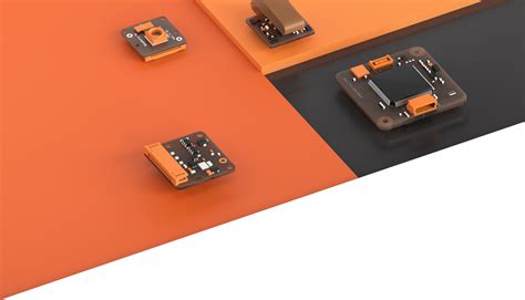
In the field of consumer electronics, Seed Fusion PCB is widely used in the manufacture of products such as smartphones, tablets, and wearable devices. Its efficiency and flexibility enable companies to quickly respond to market demand and launch new products.
2.Medical equipment
The design and manufacture of medical equipment requires extremely high reliability and precision of PCB. Seed Fusion PCB can meet these requirements and is widely used in medical monitoring equipment, diagnostic instruments and other fields.
3.Automotive electronics
With the development of automotive intelligence and electrification, the complexity of automotive electronic systems continues to increase. Seed Fusion PCB can provide high-performance circuit solutions for automotive sensors, controllers, and infotainment systems.
4.Industrial automation
In the field of industrial automation, Seed Fusion PCB is used in the manufacture of various control systems and sensors. Its high reliability and durability enable it to work stably in harsh environments.
Future development trend of Seed Fusion PCB
With the continuous advancement of science and technology, Seed Fusion PCB has broad prospects for future development.
1.Material innovation
In the future, with the continuous research and development of new conductive materials and substrates, the performance of Seed Fusion PCB will be further improved. The application of new materials will enable PCB to work stably under extreme conditions such as high temperature, high frequency and high voltage.
2.Automated production
With the advancement of Industry 4.0, the production process of Seed Fusion PCB will gradually be automated. This will further improve production efficiency, reduce labor costs, and give companies an advantage in competition.
3.Intelligent design
In the future, Seed Fusion PCB will combine artificial intelligence and big data analysis to achieve intelligent design. Through data-driven design optimization, enterprises can better meet market demand and improve product competitiveness.
4.Sustainable development
Globally, environmental protection and sustainable development have become important issues. The environmental characteristics of Seed Fusion PCB will make it occupy an important position in future electronic manufacturing and promote the industry’s transformation to green production.
Conclusion
As an emerging printed circuit board manufacturing technology, Seed Fusion PCB is changing the landscape of the electronics manufacturing industry with its high efficiency, flexibility and environmental protection. With the advancement of material technology, the promotion of production automation and the realization of intelligent design, the application field of Seed Fusion PCB will continue to expand, and its future development prospects are worth looking forward to. Through continuous innovation and optimization, Seed Fusion PCB will bring more possibilities to the design and manufacturing of electronic products and promote the progress and development of the entire industry.