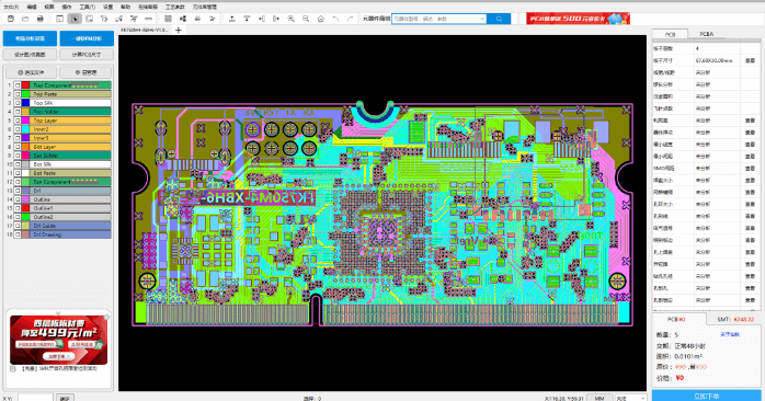
Several tests for bare PCB boards
PCB boards are called printed circuit boards in Chinese, also known as printed circuit boards and printed circuit boards. They are important electronic components.
The quality of PCBs largely determines the quality of electronic components. Therefore, in the process of producing PCB boards, detection is a very important part. Through detection, defects that affect functionality, such as open circuits and short circuits that are not easily visible, can usually be found.
For any designed product to be ultimately successful, it must be tested multiple times. Testing of PCB circuit boards can minimize major problems, find minor errors, save time and reduce overall costs.
PCB testing is mainly used to alleviate problems in the entire manufacturing process and the final production process. These types of tests can also be used on prototypes or small-scale assemblies, which helps to find potential problems that may exist in the final product.
Several ways to test bare PCB boards
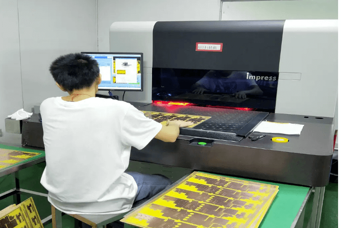
01 AOI test:
AOI automatic optical inspection equipment has been widely used in various industries. In the PCB processing process, as an important inspection equipment, key quality assurance tools are also widely used.
AOI is also called mid-test in the PCB production process. It is tested after the circuit pattern is etched out of the copper foil on the PCB board. The equipment scans the pattern on the board and compares it with the design file to distinguish the PCB board pattern status, and then compares it with the PCB board pattern data stored by the AOI itself. Defects are reported at different locations, and finally confirmed by the inspector to complete the entire inspection process.
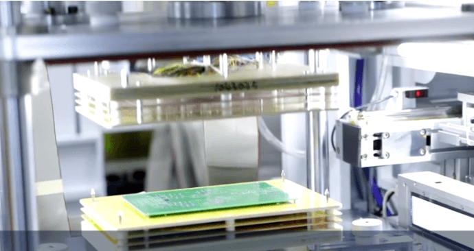
02 Flying probe test:
Flying probe test is a highly recognized and effective test form that can effectively discover production quality problems. Flying probe test has been proven by the industry to be a particularly cost-effective test method to improve circuit board standards.
Flying probe test uses two or more independent probes and operates without fixed test points. These probes are electromechanically controlled and move according to specific software instructions. Therefore, the initial cost of flying probe test is lower, and the test efficiency is not high compared to fixture test. After all, flying probe test is a test that moves the probe point by point, so it is practical for small batch orders.
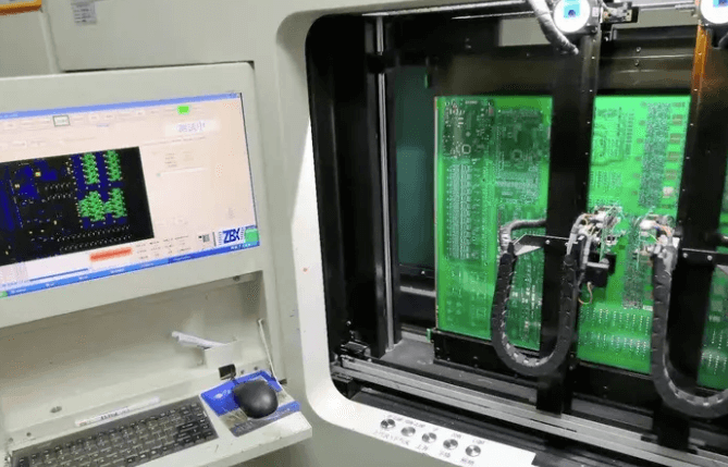
03 Jig test:
Jig is a special fixture designed with PCB as the model for electrical performance on-off test. It can be single-sided or double-sided.
PCB electrical testing first requires the production of a set of test fixtures. The metal probes of the fixtures are connected to the pads or test points on the PCB. When the PCB is powered on, the voltage and current values of the test circuit are obtained to observe whether the tested circuit is conducting normally. The advantage of using electrical testing is high test efficiency, and the disadvantage is that the cost is also high. Each PCB needs a different test fixture. Therefore, fixture testing is practical for large-volume orders.
04 Manual visual inspection:
Testing visual inspection of PCBs is the most traditional inspection method. The advantages are low initial cost and no test fixture. Visual inspection using a magnifying glass or a calibrated microscope determines whether the PCB board is qualified and determines when correction operations are required.
Visual inspection tests are only for boards with simple circuits. The disadvantages are subjective human errors, high long-term costs, discontinuous defect detection, and difficulty in data collection. With the increase in PCB production and the reduction in the wire spacing and component size on PCB, visual inspection test methods are becoming increasingly unfeasible.

PCB test fixture design
For fixture testing, positioning holes must be designed. The holes in the board must be larger than 1.5mm to be used as test positioning holes. Without positioning holes, the board will deviate during testing and the test will be inaccurate.
The role of positioning holes is the processing benchmark during the production of printed circuit boards. There are various positioning methods for PCB positioning holes, mainly based on different positioning accuracy requirements. The positioning holes on printed circuit boards should be represented by special graphic symbols. When the requirements are not high, larger assembly holes in printed circuit boards can also be used instead.
In order to facilitate the fixing of printed circuit boards when drilling and milling the shape of printed circuit boards, as well as to facilitate online testing, many circuit board factories hope that design engineers will design four non-metallized holes on the PCB. The positioning holes are usually designed as non-metallized holes with a drilling diameter of 1.5mm or 2.0mm. If the board surface is tight, at least three positioning holes should be placed and placed diagonally.
If you make a panel, you can also regard the panel as a PCB. The whole panel only needs to have three positioning holes, and the positioning holes can be placed on the process edge of the panel. If the design engineer does not place them, the circuit board manufacturer will automatically add them without affecting the circuit, or use the existing non-metallized holes in the board as positioning holes.
Case
DFM helps PCB test smoothly
Case 1

For the “adapter board” product, there is no need to fix it with screws, and the device holes in the board are also relatively small. At this time, the design engineer only designs the product according to the requirements, and does not place large holes as positioning holes for this product during design. This batch of boards cannot be tested during testing without positioning holes.
DFM detects this problem and recommends that the design engineer design positioning holes in the board, or add process edges to the panel, and design positioning holes on the process edges.
DFM helps PCB test smoothly
Case 2
For the “gold finger card board” product, the card board is inserted on a certain motherboard and does not need to be fixed with screw holes because the designed board has no positioning holes. There are no positioning holes during manufacturing, and the batch boards cannot be tested.
DFM detects this problem and recommends that the design engineer design positioning holes in the board, or add process edges to the board and design positioning holes on the process edges.
For products that do not require screw holes for fixing, design engineers also need to consider manufacturing and design positioning holes. For example, when the board space is small and positioning holes cannot be designed, the board can be designed with process edges and positioning holes can be designed on the process edges.
It is definitely right for design engineers to design products according to requirements, but what about manufacturing? The absence of positioning holes during PCB board manufacturing will bring many inconveniences to production, such as: batch boards, no positioning holes cannot be tested, and molding without positioning holes will cause the shape to be milled out of position.


