Sharing Experiences in the Process of Copying PCBs/Designing Schematics to PCBs
Introduction: Generally, creating a PCB from a copy or schematic requires relatively low technical requirements, and making a quick PCB is straightforward. However, in practice, it’s important to first clarify your goals. Of course, the key is to understand the layout and routing requirements of the components used. By properly placing the components and routing the PCB, you can ensure a high-quality PCB.
PCBs (Printed Circuit Boards), also known as printed circuit boards or printed circuit boards, are important electronic components that support and provide electrical connections for electronic components. Because they are manufactured using electronic printing techniques, they are called “printed” circuit boards. PCB copying involves using reverse engineering techniques to reverse engineer the physical electronic product and circuit board, creating a 1:1 replica of the original product’s PCB files, bill of materials (BOM), schematics, and other technical documents, as well as the PCB silkscreen production files. These technical and production files are then used to perform PCB fabrication, component soldering, flying probe testing, and circuit board debugging, ultimately completing a complete replica of the original circuit board prototype.
PCB copying, currently also referred to in the industry as circuit board copying, circuit board cloning, circuit board duplication, PCB cloning, PCB reverse design, or PCB reverse development, has various definitions within the industry and academia, but none are comprehensive. To provide a precise definition, we can refer to the definition of a leading domestic PCB copying laboratory: PCB copying involves using reverse engineering techniques to reverse engineer the circuit board, using physical electronic products and circuit boards. This involves reproducing the original product’s PCB files, bill of materials (BOM), schematics, and other technical documents, as well as the silkscreen production files, in a 1:1 replica. These technical and production files are then used to fabricate the PCB, perform component soldering, perform flying probe testing, and debug the circuit board, ultimately completing a complete replica of the original circuit board prototype. Since electronic products are controlled by various circuit boards, this process can be used to extract the complete technical data of any electronic product, allowing for the imitation and cloning of the product.
Many people misunderstand the concept of PCB copying. In fact, with the continuous development and deepening of the copying industry, the concept has expanded beyond simple circuit board duplication and cloning to encompass secondary product development and new product research and development. For example, by analyzing existing product technical documents, understanding and exploring design concepts, structural features, and process technologies, we can provide feasibility analysis and competitive references for new product development and design. This helps R&D and design teams keep pace with technological trends, adjust and improve product designs, and develop competitive new products. Furthermore, by extracting and partially modifying technical documents, PCB copying enables rapid upgrades and secondary development of various electronic products. Based on the extracted file images and schematics, designers can optimize and modify the PCB design according to customer requirements, adding new features or redesigning functional features. This allows products with new features to be launched quickly and with a fresh look, securing intellectual property rights and gaining a competitive edge in the market, bringing dual benefits to customers.
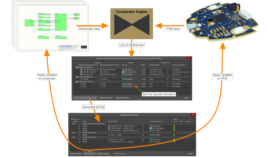
PCB copying involves cloning an existing PCB and exporting schematics. This file is then used for production. This file can also be used for secondary development and redesign based on user needs, enabling product upgrades and expansions. So, how do you go from a PCB copy schematic to a physical PCB?
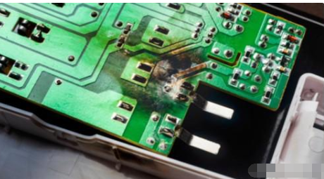
As you all know, PCB fabrication involves transforming a designed/cloned schematic into a physical PCB. Don’t underestimate this process. Many things that seem feasible in principle are difficult to implement in practice, or what some people can achieve may not be possible for others. Therefore, while making a PCB is easy, making a good one is not.
Two of the most challenging aspects of microelectronics are processing high-frequency and weak signals. This is where PCB fabrication expertise becomes crucial. The same schematic and components can produce different PCBs depending on the person creating them. So, how can you create a good PCB? Based on our experience, we’d like to share our insights on the following aspects:
1.Clarify your goals
When accepting a design/copying assignment, the first thing to do is to clearly define your goals. Whether designing a standard PCB, a high-frequency PCB, a small-signal processing PCB, or a PCB with both high-frequency and small-signal processing, if you’re only designing a standard PCB, ensuring a reasonable and neat layout and accurate mechanical dimensions is sufficient. If there are moderately loaded or long lines, appropriate measures should be taken to reduce the load, strengthen the drive of long lines, and prevent reflections. Signal lines exceeding 40MHz require special consideration, such as crosstalk. Higher frequencies impose stricter limits on trace lengths. According to distributed parameter network theory, the interaction between high-speed circuits and their connections is a crucial factor and cannot be ignored during system design. As gate transmission speeds increase, interference on signal lines increases accordingly, and crosstalk between adjacent signal lines increases proportionally. High-speed circuits typically consume significant power and dissipate significant heat, requiring significant attention when designing high-speed PCBs.
When a board carries weak signals in the millivolt or even microvolt range, these signal lines require special attention. Because they are so weak, small signals are easily interfered with by other stronger signals. Shielding measures are often necessary, as otherwise the signal-to-noise ratio will be significantly reduced. Consequently, the useful signal is drowned out by noise and cannot be effectively extracted.
Board commissioning and testing must also be considered during the design phase. Factors such as the physical location and isolation of test points must be considered, as some small and high-frequency signals cannot be directly measured with a probe.
Additionally, other factors should be considered, such as the number of board layers, the package size of the components used, and the mechanical strength of the board. Before designing a PCB, it’s important to have a clear understanding of the design goals.
2.Understand the Layout Requirements of the Component Functions
We know that some specialized components have unique layout requirements. For example, the analog signal amplifiers used in LOTI and APH require a stable power supply with low ripple. The analog small signal components should be kept as far away from power devices as possible. On the OTI board, the small-signal amplifier section is shielded to block stray electromagnetic interference. The GLINK chip used on the NTOI board utilizes an ECL process, which consumes high power and generates significant heat. Therefore, special consideration must be given to heat dissipation during layout. If natural cooling is used, the GLINK chip should be placed in an area with good air circulation, and the heat dissipated should not significantly affect other chips. If speakers or other high-power devices are installed on the board, the potential for serious power supply pollution should also be taken into account.
3. Component Layout Considerations
The primary consideration in component layout is electrical performance. Components with closely connected wiring should be placed together whenever possible. High-speed wiring, in particular, should be kept as short as possible during layout, and power signals and small-signal components should be separated. While ensuring circuit performance, component placement should also be considered, ensuring neat and aesthetically pleasing layout for ease of testing. The board’s mechanical dimensions and socket placement also require careful consideration.
Grounding and transmission delay on interconnects in high-speed systems are also primary considerations during system design. Signal line transmission time significantly impacts overall system speed, especially for high-speed ECL circuits. Although the integrated circuit itself is very fast, the added delay introduced by conventional interconnects on the backplane (approximately 2ns of delay per 30cm of line length) can significantly reduce system speed. Synchronous components such as shift registers and synchronous counters placed on the same board can cause errors in the shift registers due to unequal transmission delays of clock signals to different boards. If these components cannot be placed on the same board, the length of the clock lines from the common clock source to each board must be equal where synchronization is critical.
4. Wiring Considerations
With the completion of OTNI and star fiber optic network designs, there will be an increasing number of boards with high-speed signal lines exceeding 100MHz that will require design. Here, we will introduce some basic concepts of high-speed lines.
1.Transmission Lines
Any “long” signal path on a printed circuit board can be considered a transmission line. If the transmission delay of this line is much shorter than the signal rise time, reflections generated during the signal rise time will be overwhelmed. Overshoot, kickback, and ringing no longer occur. For most current MOS circuits, the ratio of rise time to line propagation delay is much greater, allowing trace lengths to be measured in meters without signal distortion. However, for faster logic circuits, particularly ultra-high-speed ECL circuits, trace lengths must be significantly shortened to maintain signal integrity due to the increasing edge speeds.
There are two methods for enabling high-speed circuits to operate on relatively long traces without significant waveform distortion. TTL uses Schottky diode clamping for fast falling edges, clamping overshoot to a level one diode drop below ground, thus reducing the subsequent kickback. Slower rising edges allow for overshoot, but this is attenuated by the relatively high output impedance (50-80Ω) of the circuit in the “H” state. Furthermore, due to the greater noise immunity of the “H” state, the kickback problem is less prominent. For HCT series devices, combining Schottky diode clamping with series resistor termination can significantly improve the performance.
When fanning out along signal lines, at higher bit rates and faster edge rates, the TTL shaping methods described above become somewhat inadequate. This is because reflected waves in the lines tend to combine at high bit rates, causing severe signal distortion and reduced interference immunity. Therefore, to address reflections, another approach is commonly used in ECL systems: line impedance matching. This method controls reflections and ensures signal integrity.
Strictly speaking, transmission lines are not strictly necessary for conventional TTL and CMOS devices with slower edge rates. They are also not always necessary for high-speed ECL devices with faster edge rates. However, when used, transmission lines offer the advantages of predictable line delays and impedance matching to control reflections and oscillations. 1
There are five basic factors that determine whether to use transmission lines. They are: (1) the edge rate of the system signal, (2) the connection distance, (3) the capacitive load (the amount of fan-out), (4) the resistive load (the termination method of the line); (5) the allowable backlash and overshoot percentage (the degree of reduction in AC interference immunity).
2.Several types of transmission lines
(1) Coaxial cable and twisted pair: They are often used to connect between systems. The characteristic impedance of coaxial cable is usually 50Ω and 75Ω, and the twisted pair is usually 110Ω.
(3) Microstrip line on printed circuit board
Microstrip line is a strip conductor (signal line). It is separated from the ground plane by a dielectric. If the thickness, width and distance between the line and the ground plane are controllable, its characteristic impedance can also be controlled.
(3) Stripline on printed circuit board
Stripline is a copper strip line placed in the middle of a dielectric between two conductive planes. If the thickness and width of the line, the dielectric constant of the medium, and the distance between two conductive planes are controllable, then the characteristic impedance of the line can also be controlled.
Similarly, the transmission delay per unit length of a stripline is independent of the line width or spacing; it depends solely on the relative dielectric constant of the medium used.
3.Terminating Transmission Lines
When a line is terminated at the receiving end with a resistor equal to the line’s characteristic impedance, the line is called a parallel-terminated transmission line. This is primarily used to improve electrical performance, including driving distributed loads.
Sometimes, to save power, a 104Ω capacitor is connected in series with the terminating resistor to form an AC termination circuit, which effectively reduces DC losses.
Connecting a resistor in series between the driver and the transmission line, without a terminating resistor at the end of the line, is called series termination. Overshoot and ringing on longer lines can be controlled using series damping or series termination techniques. Series damping is achieved by placing a small resistor (typically 10-75Ω) in series with the output of the driver gate. This damping method is suitable for use with lines whose characteristic impedance is controlled (such as chassis traces, circuit boards without a ground plane, and most wire wrap).
With series termination, the sum of the series resistance and the output impedance of the circuit (driver gate) equals the characteristic impedance of the transmission line. Series-terminated lines have the disadvantage of only being able to use lumped loads at the end and having longer transmission delays. However, this can be overcome by using redundant series-terminated transmission lines.
4.Unterminated Transmission Lines
If the line delay is much shorter than the signal rise time, the transmission line can be used without series or parallel termination. If the round-trip delay (the time it takes for the signal to travel back and forth on the transmission line) of an unterminated line is shorter than the rise time of the pulse signal, the kickback caused by the unterminated line is approximately 15% of the logic swing. The open line length is approximately:
Lmax
Where: tr is the rise time
tpd is Transmission Delay per Unit Line Length
5.Comparison of Several Termination Methods
Both parallel and series termination have their own advantages. The decision to use one or both depends on the designer’s preference and system requirements. The primary advantages of parallel termination are high system speed and complete, distortion-free signal transmission along the line. Loads on long lines do not affect the transmission delay of the gate driving the long line, nor do they affect the edge speed of the signal, but they do increase the transmission delay of the signal along the line. When driving a large fan-out, the load can be distributed along the line using short branch lines, rather than being lumped together at the end of the line as in series termination.
Series termination enables a circuit to drive several parallel load lines. The incremental delay caused by capacitive loading in series termination is approximately twice that of the corresponding parallel termination. Capacitive loading in short lines slows edge speeds and increases gate delay. However, series terminationThe crosstalk of the wiring is smaller than that of the parallel terminal wiring. The main reason is that the signal amplitude transmitted along the series terminal wiring is only half of the logic swing, so the switching current is only half of the switching current of the parallel terminal. The smaller the signal energy, the smaller the crosstalk.
6. PCB board wiring technology
Whether to use a double-sided board or a multi-layer board when making a PCB depends on the operating frequency, the complexity of the circuit system and the requirements for assembly density. When the clock frequency exceeds 200MHZ, a multi-layer board is used. If the operating frequency exceeds 350MHz, a printed circuit board with polytetrafluoroethylene as the dielectric layer is used because it has smaller high-frequency attenuation, smaller parasitic capacitance, faster transmission speed, and saves power due to its larger Z0. The following principles are required for the routing of the printed circuit board
(1) All parallel signal lines should be spaced as far as possible to reduce crosstalk. If there are two signal lines that are close to each other, a ground line should be run between the two lines to provide shielding. (2) When designing signal transmission lines, avoid sharp turns to prevent reflections caused by sudden changes in the characteristic impedance of the transmission line. Try to design it into a uniform arc line with a certain size. The width of the printed circuit board can be calculated based on the above-mentioned calculation formula for the characteristic impedance of the microstrip line and the strip line. The characteristic impedance of the microstrip line on the printed circuit board is generally between 50 and 120Ω. In order to obtain a large characteristic impedance, the line width must be made very narrow. However, very thin lines are not easy to make. Considering various factors, it is generally appropriate to choose an impedance value of about 68Ω, because choosing a characteristic impedance of 68Ω can achieve a balance between delay time and power consumption. A 50Ω transmission line will consume more power; a larger impedance can certainly reduce power consumption, but it will increase the transmission delay time. Since negative line capacitance will cause the transmission delay time to increase and the characteristic impedance to decrease. However, the intrinsic capacitance per unit length of a line segment with very low characteristic impedance is relatively large, so the transmission delay time and characteristic impedance are less affected by the load capacitance. An important feature of a properly terminated transmission line is that the branch short line should have little effect on the line delay time. When Z0 is 50Ω, the length of the branch short line must be limited to within 2.5cm. To avoid large ringing.
(4) For double-sided boards (or four-layer lines in a six-layer board), the lines on both sides of the circuit board should be perpendicular to each other to prevent mutual induction and crosstalk.
(5) If the printed circuit board is equipped with high-current devices, such as relays, indicator lights, speakers, etc., their ground lines should be separated and routed separately to reduce noise on the ground lines. The ground lines of these high-current devices should be connected to an independent ground bus on the plug-in board and the backplane, and these independent ground lines should also be connected to the ground point of the entire system.
(6) If there is a small signal amplifier on the board, the weak signal line before amplification should be kept away from the strong signal line, and the line should be as short as possible. If possible, it should be shielded with a ground line.
The following is the PCB copy process:
Step 1: Get a PCB and first write down the model, parameters, and position of all components on paper, especially the direction of the diodes and three-tubes and the direction of the IC gap.
Step 2: Remove all components and remove the tin from the pad holes. Clean the PCB with alcohol, then place it in a scanner. Launch Photoshop and scan the silkscreened surface in color. Print it out for future use.
Step 3: Lightly sand the top and bottom layers with gauze paper until the copper coating is shiny. Place the PCB in a scanner, launch Photoshop, and scan each layer in color.
Step 4: Adjust the contrast and brightness of the canvas to create a sharp contrast between the copper-coated and non-coated areas. Then convert the image to black and white and check for clarity. If not, repeat this step. If so, save the image as black and white BMP files, TOP.BMP and BOT.BMP.
Step 5: Convert the two BMP files to ProTEL and import the two layers into ProTEL. If the pads and vias on both layers are roughly aligned, the previous steps have been successful. If not, repeat step 3.
Step 6: , convert the TOP.BMP file to TOP.PCB and place the components according to the drawing in step 2.
Step 7: , convert the BOT.BMP file to BOT.PCB.
Step 8: import the TOP.PCB and BOT.PCB files into PROTEL and combine them into a single drawing.
Step 9: use a laser printer to print the TOP LAYER and BOTTOM LAYER onto transparent film (1:1 ratio). Place the film on the PCB and compare to see if there are any errors.