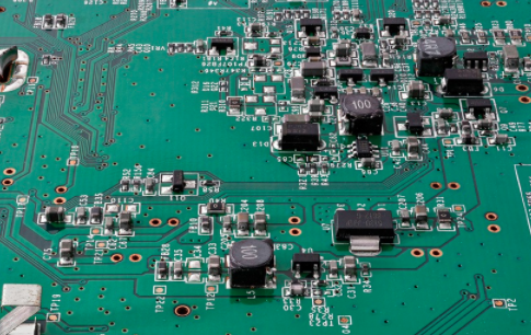
Sharing three tips on PCB design experience
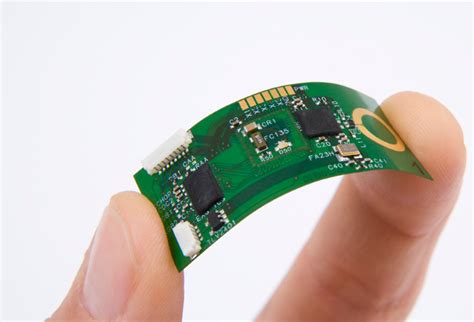
PCB is like the skeleton and nerve network of electronic circuits, and plays a vital role in electronic engineering projects, but many people do not know or do not know enough about PCB design. In fact, there are many fun things in PCB design, and only by practicing can you have a deep understanding.
When I was in college, I was particularly interested in circuit board design and hardware circuit design, and I studied it seriously. At that time, I thought it would be great to find a job sitting in an office doing computer drawing after graduation. After graduation, I also entered an automotive electronics company in Dongguan as I wished, and engaged in electronic research and development work, including making BOM tables, prototype debugging and PCB drawing work. When I graduated in 2002, there was no such job as PCB engineer. Basically, I had to know a little bit about everything, including schematic drawing, device selection, PCB drawing, sample welding, debugging, BOM production, work instructions, etc., and I embarked on the road of electronic research and development.
01 Schematic diagram
Although a good schematic diagram cannot guarantee good wiring, good wiring starts with a good schematic diagram. Be thoughtful when drawing schematics, and be sure to consider the signal flow of the entire circuit. If you have a normal and stable signal flow from left to right in the schematic, you should have the same good signal flow on the PCB. Give as much useful information as possible on the schematic.
Because sometimes the circuit design engineer is not here, customers will ask us to help solve circuit problems, and designers, technicians, and engineers who do this work will be very grateful, including us. In addition to the usual reference identifiers, power consumption and error tolerances, what other information should be given in the schematic? Here are some suggestions to turn ordinary schematics into first-class schematics. Add waveforms, mechanical information about the housing, trace lengths, and blank areas; indicate which components need to be placed on the PCB; give adjustment information, component value ranges, heat dissipation information, controlled impedance traces, comments, concise circuit action descriptions… (and others).
02 Don’t trust anyone
If you don’t design the wiring yourself, be sure to leave plenty of time to carefully check the wiring person’s design. A little prevention is worth a hundred times the remedy at this point. Don’t expect the wiring person to understand your ideas. Your opinions and guidance are important at the beginning of the wiring design process. The more information you can provide and the more involved you are in the entire wiring process, the better the resulting PCB will be. Set a tentative completion point for the wiring design engineer-quickly check according to the wiring progress you want. This “closed loop” method can prevent the wiring from going astray, thereby minimizing the possibility of rework.
Instructions that need to be given to the wiring engineer include: a brief description of the circuit function, a PCB outline indicating the input and output locations, PCB stacking information (for example, how thick the board is, how many layers there are, and detailed information on each signal layer and ground plane-power consumption, ground, analog signals, digital signals, and RF signals); which signals are needed on each layer; where important components are required; the exact location of bypass components; which traces are important; which lines require controlled impedance traces; which lines need to match lengths; the size of the components; which traces need to be kept away from (or close to) each other; which lines need to be kept away from (or close to) each other; which components need to be kept away from (or close to) each other; which components should be placed on the top of the PCB and which ones should be placed below. Never complain about having too much information to give someone – too little? Yes; too much? No.
A learning experience: About 10 years ago, I designed a multi-layer surface mount circuit board – there were components on both sides of the board. The board was fixed in a gold-plated aluminum housing with many screws (because of strict shock protection specifications). The pin that provided bias feedthrough went through the board. The pin was connected to the PCB with a solder wire.
It was a complicated device. Some of the components on the board were used for test settings (SAT). But I had clearly defined the location of these components. Can you guess where these components were installed? That’s right, on the bottom of the board. The product engineers and technicians were not happy when they had to take the whole device apart, complete the settings, and then put it back together. I have never made this mistake since.
03 Position
Just as in the PCB, position is everything. Where to place a circuit on the PCB, where to install its specific circuit components, and what other circuits are adjacent to it are all very important.
Usually, the positions of input, output and power are predetermined, but the circuits between them need to be “creative”. That’s why paying attention to wiring details will pay huge dividends. Start with the position of key components and consider them according to the specific circuit and the entire PCB. Specifying the position of key components and the path of signals from the beginning helps ensure that the design achieves the expected working goals. Getting the right design can reduce costs and stress – thus shortening the development cycle.
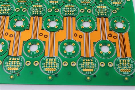
In addition, let’s talk about those “special pads” on the PCB board
, teardrop pad

Teardrop is a drip connection between the pad and the wire or the wire and the guide hole. The purpose of setting teardrops is to avoid disconnection of the contact point between the wire and the pad or the wire and the guide hole when the circuit board is impacted by a huge external force. In addition, setting teardrops can also make the PCB circuit board look more beautiful.
The role of teardrop is to avoid reflection caused by a sudden decrease in signal line width, and to make the connection between the trace and the component pad tend to be smooth and transitional, solving the problem of easy breakage of the connection between the pad and the trace.
- In welding, it can protect the pad and avoid the pad from falling off due to multiple welding
- Enhance the reliability of the connection (production can avoid uneven etching, cracks caused by offset vias, etc.)
- Smooth impedance and reduce sharp impedance jumps
In circuit board design, in order to make the pad stronger and prevent the pad and the wire from being disconnected during mechanical board making, a transition zone is often arranged between the pad and the wire with copper film, which is shaped like a teardrop, so it is often called a teardrop
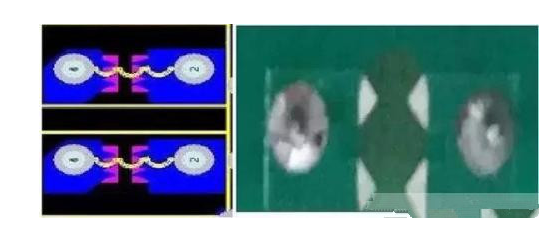
The second one is the discharge tooth
wKgZomWJOPiAI_I8AAHPc7R7_dM276.png
This thing is called a discharge tooth, a discharge gap or a spark gap. Spark gaps are used. Spark gaps are a pair of triangles pointing to opposite acute angles, with the fingertips 10mil and 6mil apart. One triangle is grounded and the other is connected to the signal line. This triangle is not a component, but is made by using a copper foil layer during the PCB wiring process. These triangles need to be set on the top layer (componentside) of the PCB board and cannot be covered by solder mask.
- During the switching power supply surge test or ESD test, high voltage will be generated at both ends of the common mode inductor, and arcing will occur. If the distance to the surrounding devices is close, the surrounding devices may be damaged. Therefore, a discharge tube or varistor can be connected in parallel to it to limit its voltage, thereby playing the role of arc extinguishing. Placing lightning protection devices is very effective but the cost is relatively high.
- Another way is to add discharge teeth at both ends of the common mode inductor during PCB design, so that the inductor discharges through the two discharges, avoiding discharge through other paths, thereby reducing the impact on surrounding and subsequent devices.
The discharge gap does not require additional costs and can be drawn when drawing the PCB board. However, it should be noted that this type of discharge gap is an air-type discharge gap and can only be used in environments where ESD is occasionally generated. If used in situations where ESD often occurs, carbon deposits will form at two triangular points between the discharge gaps due to frequent discharges, causing a short circuit in the discharge gap and a short circuit of the signal line to the ground, thereby causing system failure.