Signal Integrity Issues in PCB Design: Analysis and Solutions
Abstract
Signal Integrity (SI) is a critical aspect of high-speed PCB design, affecting the performance and reliability of electronic systems. As data rates increase and signal rise times decrease, maintaining signal integrity becomes more challenging. This paper explores common SI issues in PCB design, including impedance mismatches, crosstalk, reflections, and power integrity problems. Additionally, mitigation techniques such as proper termination, controlled impedance routing, and power distribution network (PDN) optimization are discussed. By understanding these challenges and implementing best practices, designers can ensure robust signal transmission in high-speed circuits.
1. Introduction
With the increasing demand for high-speed digital communication, PCB designers face significant challenges in maintaining signal integrity. Signal Integrity (SI) refers to the quality of electrical signals as they propagate through transmission lines, ensuring minimal distortion, noise, and timing errors. Poor SI can lead to data corruption, electromagnetic interference (EMI), and system failures.
This paper examines key SI issues in PCB design, their root causes, and effective countermeasures. The discussion covers transmission line effects, crosstalk, reflections, and power integrity concerns, followed by practical design solutions.
2. Common Signal Integrity Issues in PCB Design
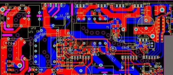
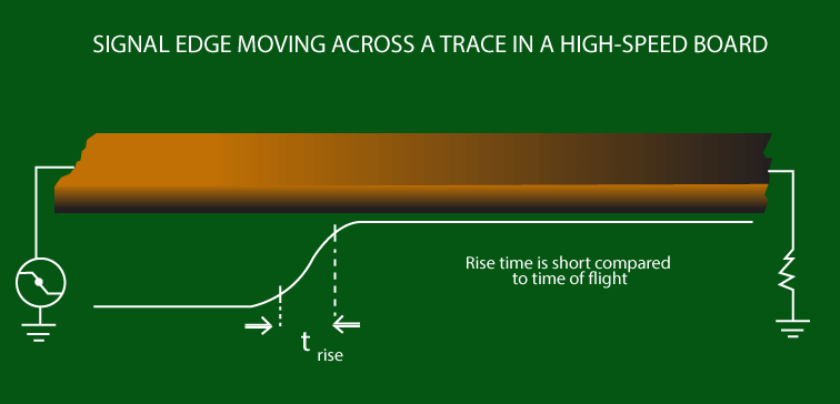
2.1 Impedance Mismatch and Reflections
Impedance mismatch occurs when the characteristic impedance of a transmission line does not match the source or load impedance. This leads to signal reflections, causing overshoot, undershoot, and ringing.
Causes:
- Improper trace width or dielectric thickness affecting impedance.
- Discontinuities such as vias, connectors, or stubs.
- Incorrect termination techniques.
Effects:
- Increased bit error rates (BER) in high-speed signals.
- Signal distortion leading to timing violations.
Solutions:
- Use controlled impedance routing (e.g., microstrip or stripline).
- Implement proper termination (series, parallel, or AC termination).
- Minimize via stubs and optimize return paths.
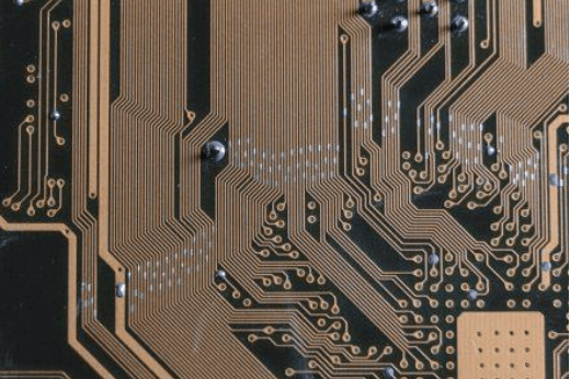
2.2 Crosstalk (Near-End and Far-End)
Crosstalk is unwanted coupling between adjacent traces, categorized as:
- Near-End Crosstalk (NEXT): Coupling near the signal source.
- Far-End Crosstalk (FEXT): Coupling at the receiver end.
Causes:
- Parallel routing of high-speed traces over long distances.
- Insufficient spacing between traces.
- High edge rates (fast rise/fall times).
Effects:
- Induced noise degrading signal quality.
- False triggering in digital circuits.
Solutions:
- Follow the 3W rule (trace spacing ≥ 3× trace width).
- Use differential signaling for noise immunity.
- Implement ground shielding between critical traces.
2.3 Power Integrity and Ground Bounce
Power integrity issues arise when the power delivery network (PDN) fails to provide stable voltage levels, leading to:
- Ground bounce: Voltage fluctuations in the ground plane due to simultaneous switching noise (SSN).
- Power supply noise: Ripple and droop affecting signal quality.
Causes:
- High current transients in digital ICs.
- Poor decoupling capacitor placement.
- High PDN impedance at key frequencies.
Effects:
- Increased jitter and timing errors.
- Logic failures in sensitive circuits.
Solutions:
- Optimize decoupling capacitor placement (low-ESR MLCCs).
- Use power and ground planes for low-impedance return paths.
- Perform PDN analysis using simulation tools.
2.4 EMI and Radiated Noise
Electromagnetic interference (EMI) can degrade SI by introducing external noise or radiating unwanted signals.
Causes:
- High-frequency signal loops.
- Poor grounding techniques.
- Unshielded high-speed traces.
Effects:
- Regulatory compliance failures.
- Signal degradation in sensitive analog circuits.
Solutions:
- Implement proper grounding (star grounding, split planes).
- Use EMI shielding and ferrite beads.
- Minimize loop areas in high-speed signal paths.

3. Simulation and Measurement Techniques
3.1 Time-Domain Reflectometry (TDR)
TDR helps identify impedance discontinuities by analyzing reflected waveforms.
3.2 Eye Diagram Analysis
Eye diagrams assess signal quality in high-speed links, revealing jitter, noise, and intersymbol interference (ISI).
3.3 S-Parameter Modeling
S-parameters characterize high-frequency behavior, aiding in impedance matching and crosstalk analysis.
4. Best Practices for SI Optimization
- Controlled Impedance Routing: Match trace impedance to system requirements.
- Proper Termination: Use series or parallel termination to minimize reflections.
- Minimize Crosstalk: Increase spacing, use guard traces, and avoid parallel routing.
- Optimize Power Delivery: Use low-inductance decoupling networks.
- Simulate Early: Leverage SI tools (HyperLynx, ADS, Sigrity) for pre-layout analysis.
5. Conclusion
Signal Integrity is a critical factor in modern PCB design, especially for high-speed applications. By understanding common SI issues such as reflections, crosstalk, and power integrity problems, designers can implement effective mitigation strategies. Proper simulation, controlled impedance routing, and optimized power distribution are essential for ensuring reliable signal transmission. Future advancements in materials and design methodologies will further enhance SI performance in next-generation PCBs.