Similarities between analog and digital routing strategies
1.1 Bypass or decoupling capacitors
Both analog and digital devices require these types of capacitors when routing. They all require a capacitor close to their power pins, which is usually 0.1mF. Another type of capacitor is required on the system power supply side, which is usually about 10mF.
The capacitance range is between 1/10 and 10 times the recommended value. However, the pins must be short and as close to the device (for 0.1mF capacitors) or the power supply (for 10mF capacitors) as possible.
Adding bypass or decoupling capacitors to the circuit board and the location of these capacitors on the board are common sense for both digital and analog designs. But interestingly, the reasons are different. In analog routing design, bypass capacitors are usually used to bypass high-frequency signals on the power supply. If bypass capacitors are not added, these high-frequency signals may enter sensitive analog chips through the power supply pins. Generally speaking, the frequency of these high-frequency signals exceeds the ability of analog devices to suppress high-frequency signals. If bypass capacitors are not used in analog circuits, noise may be introduced into the signal path, and in more serious cases, vibration may even be caused.
In analog and digital PCB design, bypass or decoupling capacitors (1mF) should be placed as close to the device as possible. Power supply decoupling capacitors (10mF) should be placed at the power line entrance of the circuit board. In all cases, the pins of these capacitors should be short
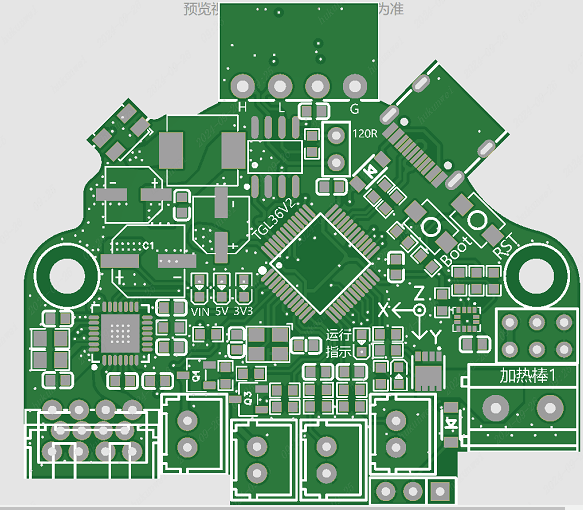
On this circuit board, different routes are used to lay power and ground lines. Due to this improper matching, the electronic components and lines of the circuit board are more likely to be affected by electromagnetic interference
3 In this single-sided board, the power and ground lines to the devices on the circuit board are close to each other. The matching of power and ground lines in this circuit board is more appropriate than that in Figure 2. The possibility of electromagnetic interference (EMI) of electronic components and lines in the circuit board is reduced by 679/12.8 times or about 54 times

For digital devices such as controllers and processors, decoupling capacitors are also needed, but for different reasons.
One function of these capacitors is to act as a “micro” charge reservoir. In digital circuits, large currents are usually required to perform switching of gate states. Because switching transients are generated on the chip and flow through the board during switching, it is beneficial to have extra “spare” charge. If there is not enough charge when performing the switching action, the power supply voltage will change significantly. Large voltage changes can cause digital signal levels to enter an uncertain state and may cause the state machine in the digital device to operate incorrectly. The switching current flowing through the board traces will cause voltage changes. The board traces have parasitic inductance, which can be calculated using the following formula: V = LdI/dt
Where V = change in voltage; L = board trace inductance; dI = change in current flowing through the trace; dt = time of current change.
Therefore, for many reasons, it is a good practice to apply bypass (or decoupling) capacitors at the power supply or at the power pins of active devices.
1.2 Power and ground lines should be laid together
Good coordination of the positions of power and ground lines can reduce the possibility of electromagnetic interference. If the power and ground lines are not coordinated properly, system loops will be designed and noise is likely to be generated. An example of a PCB design with improper power and ground lines is shown in Figure 2.
On this circuit board, the designed loop area is 697cm2. Using the method shown in Figure 3, the possibility of radiated noise on or off the circuit board inducing voltage in the loop can be greatly reduced.
2 Differences in routing strategies in analog and digital domains
2.1 Ground plane is a problem
The basics of circuit board routing apply to both analog and digital circuits. A basic rule of thumb is to use an uninterrupted ground plane, which reduces the dI/dt (current change over time) effect in digital circuits, which changes the ground potential and allows noise to enter the analog circuit. The routing techniques for digital and analog circuits are basically the same, except for one thing. For analog circuits, another point to note is to keep the digital signal lines and loops in the ground plane as far away from the analog circuit as possible. This can be achieved by connecting the analog ground plane separately to the system ground connection terminal or placing the analog circuit at the farthest end of the circuit board, that is, the end of the line. This is done to keep the signal path to the minimum external interference. This is not necessary for digital circuits, which can tolerate a lot of noise on the ground plane without problems.
Figure 4 (left) Isolate digital switching action from analog circuits and separate the digital and analog parts of the circuit. (right) Separate high and low frequencies as much as possible, and place high-frequency components close to the connectors on the circuit board
Figure 5 When two traces are placed close to each other on a PCB, parasitic capacitance is easily formed. Due to the existence of this capacitance, a rapid voltage change on one trace can generate a current signal on the other trace
Figure 6 If you do not pay attention to the placement of traces, traces in the PCB may generate line inductance and mutual inductance. This parasitic inductance is very harmful to the operation of circuits containing digital switching circuits
2.2 Component Location
As mentioned above, in every PCB design, the noisy part and the “quiet” part (non-noise part) of the circuit should be separated. Generally speaking, digital circuits are “rich” in noise and are not sensitive to noise (because digital circuits have a larger voltage noise tolerance); in contrast, the voltage noise tolerance of analog circuits is much smaller. Of the two, analog circuits are the most sensitive to switching noise. In the wiring of mixed-signal systems, these two circuits should be separated, as shown in Figure 4.
2.3 Parasitic Elements Generated by PCB Design
Two basic parasitic elements that can easily cause problems are formed in PCB design: parasitic capacitance and parasitic inductance. When designing a board, placing two traces close to each other will generate parasitic capacitance. This can be done by placing one trace on top of the other on two different layers or by placing one trace next to the other on the same layer, as shown in Figure 5. In both trace configurations, the change in voltage over time (dV/dt) on one trace can generate a current on the other trace. If the other trace is high impedance, the current generated by the electric field will be converted to voltage.
Fast voltage transients most often occur on the digital side of analog signal design.
If the traces where fast voltage transients occur are close to high impedance analog traces, this error will seriously affect the accuracy of the analog circuit. In this environment, analog circuits have two disadvantages: their noise tolerance is much lower than that of digital circuits; and high impedance traces are more common.
This phenomenon can be reduced by using one of the following two techniques
. The most common technique is to change the size between traces according to the equation of capacitance. The most effective dimension to change is the distance between the two traces. It should be noted that the variable d is in the denominator of the capacitance equation, and as d increases, the capacitive reactance decreases. Another variable that can be changed is the length of the two traces. In this case, as the length L decreases, the capacitive reactance between the two traces will also decrease.
Another technique is to run a ground wire between the two traces.
The ground wire is low impedance, and adding such an additional trace will weaken the electric field that generates interference,
The principle of parasitic inductance in a circuit board is similar to the principle of parasitic capacitance.
Also run two traces, one on top of the other on different layers; or one on the same layer, place one next to the other, as shown in Figure 6. In both trace configurations, the change in current over time (dI/dt) on one trace will generate a voltage on the same trace due to the inductive reactance of this trace; and a proportional current on the other trace due to the existence of mutual inductance. If the voltage change on the first trace is large enough, the interference may reduce the voltage tolerance of the digital circuit and produce errors. This phenomenon is not unique to digital circuits, but it is more common in digital circuits because of the large instantaneous switching currents in digital circuits.
To eliminate potential noise from EMI sources, it is best to separate “quiet” analog lines from noisy I/O ports. To achieve low-impedance power and ground networks, the inductive reactance of digital circuit wires should be minimized and the capacitive coupling of analog circuits should be minimized.

3 Conclusion
After the digital and analog ranges are determined, careful routing is essential to a successful PCB. Routing strategies are usually introduced as a rule of thumb because it is difficult to test the ultimate success of a product in a laboratory environment. Therefore, although there are similarities in the routing strategies of digital and analog circuits, it is still necessary to recognize and take seriously the differences in their routing strategies.


