Smart Home PCB: Design, Applications, and Future Trends
Introduction
The rapid advancement of Internet of Things (IoT) technology has revolutionized modern living, with smart homes becoming increasingly popular. At the heart of these intelligent systems lies the Printed Circuit Board (PCB), which serves as the foundation for connectivity, automation, and control in smart home devices. This article explores the role of PCBs in smart home technology, their design considerations, key applications, and future trends.
1. The Role of PCBs in Smart Home Systems
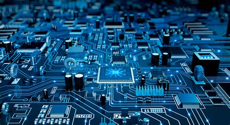
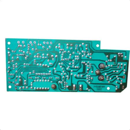
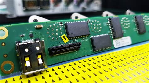
PCBs are essential components in smart home devices, enabling functionalities such as wireless communication, sensor integration, and power management. They provide a compact and efficient way to interconnect electronic components, ensuring seamless operation. Key roles of PCBs in smart homes include:
- Signal Processing: PCBs facilitate data transmission between sensors, controllers, and actuators.
- Power Management: They regulate and distribute power efficiently across devices.
- Connectivity: Embedded Wi-Fi, Bluetooth, Zigbee, and Z-Wave modules allow smart devices to communicate.
- Miniaturization: Advanced PCB designs enable smaller, more efficient smart home gadgets.
2. Key Design Considerations for Smart Home PCBs
Designing PCBs for smart home applications requires careful planning to ensure reliability, efficiency, and scalability. Some critical factors include:
2.1. Layer Stackup and Material Selection
- Multi-layer PCBs are often used to accommodate complex circuits in compact spaces.
- High-frequency materials (e.g., Rogers or FR4) are chosen for wireless communication modules.
- Flexible PCBs may be used in wearable smart home devices.
2.2. Power Efficiency and Thermal Management
- Low-power components (e.g., ARM Cortex-M microcontrollers) extend battery life in wireless devices.
- Proper heat dissipation techniques (e.g., thermal vias, heatsinks) prevent overheating.
2.3. Wireless Connectivity Integration
- Wi-Fi/Bluetooth Modules: Enable remote control via smartphones.
- Zigbee/Z-Wave: Used for low-power, mesh-network-based smart home systems.
- Antenna Design: Proper placement minimizes interference and maximizes signal strength.
2.4. Security Considerations
- Encryption Chips: Protect data from cyber threats.
- Secure Bootloaders: Prevent unauthorized firmware modifications.
2.5. Compliance with Industry Standards
- FCC/CE Certification: Ensures electromagnetic compatibility (EMC).
- IoT Security Standards: Such as IEEE 802.15.4 for Zigbee devices.
3. Applications of PCBs in Smart Home Devices
Smart home PCBs are used in a variety of applications, enhancing convenience, security, and energy efficiency.
3.1. Smart Lighting Systems
- PCBs in smart bulbs integrate LED drivers, wireless controllers, and ambient light sensors.
- Dimmable and color-changing LEDs are controlled via mobile apps or voice assistants.
3.2. Home Security and Surveillance
- Smart Cameras: Use PCBs with image sensors, motion detection, and cloud connectivity.
- Smart Locks: Incorporate fingerprint sensors, NFC, and encrypted communication.
3.3. Climate Control and HVAC Systems
- Smart Thermostats: Rely on PCBs with temperature sensors, Wi-Fi modules, and adaptive algorithms.
- Air Quality Monitors: Use gas sensors and particulate matter detectors.
3.4. Voice-Activated Assistants
- Amazon Echo & Google Home: Utilize high-performance PCBs with microphones, speakers, and AI chips.
3.5. Energy Management Systems
- Smart Plugs & Meters: Monitor and optimize electricity usage via embedded current sensors.
4. Emerging Trends in Smart Home PCB Technology
The future of smart home PCBs is shaped by advancements in IoT, AI, and sustainable electronics.
4.1. AI-Enhanced PCBs
- Edge AI Processors: Enable local data processing for faster response times.
- Machine Learning Algorithms: Improve predictive maintenance in smart appliances.
4.2. 5G and Faster Wireless Protocols
- 5G-Compatible PCBs: Support ultra-low latency for real-time automation.
- Matter Protocol: A unified IoT standard improving cross-brand compatibility.
4.3. Flexible and Wearable Electronics
- Stretchable PCBs: For smart clothing and health-monitoring devices.
4.4. Sustainable and Recyclable PCBs
- Biodegradable Substrates: Reduce electronic waste.
- Energy Harvesting: Solar-powered or kinetic-energy-based smart home sensors.
5. Challenges in Smart Home PCB Development
Despite advancements, several challenges persist:
- Interference Issues: Dense IoT networks may cause signal conflicts.
- Security Vulnerabilities: Hackers can exploit weak encryption in low-cost devices.
- High Development Costs: Advanced PCBs require expensive materials and testing.
6. Conclusion
PCBs are the backbone of smart home technology, enabling seamless automation, connectivity, and intelligence. As IoT continues to evolve, PCB designs will become more sophisticated, integrating AI, faster wireless protocols, and sustainable materials. Engineers must focus on power efficiency, security, and scalability to meet the growing demands of smart homes.
The future of smart living depends on innovative PCB solutions—making homes safer, more efficient, and truly intelligent.
This article covers the essentials of Smart Home PCBs, from design principles to future advancements. Would you like any sections expanded or additional technical details included?