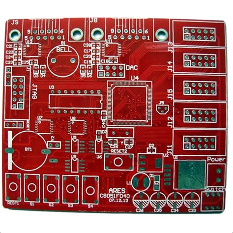
Smd pcb assembly
Benefits Of SMD PCB Assembly In Modern Electronics
Surface Mount Device (SMD) PCB assembly has revolutionized the electronics industry, offering numerous advantages that have made it the preferred method for manufacturing modern electronic devices.
One of the primary benefits of SMD PCB assembly is its ability to significantly reduce the size and weight of electronic components.
By allowing components to be mounted directly onto the surface of the printed circuit board (PCB), SMD technology eliminates the need for through-hole connections, which traditionally required more space and added bulk. This miniaturization is crucial in the development of compact and portable electronic devices, such as smartphones, tablets, and wearable technology.
In addition to size and weight reduction, SMD PCB assembly enhances the performance and reliability of electronic devices.
The shorter lead lengths in SMD components result in lower inductance and resistance, which in turn improves the overall electrical performance. This is particularly important in high-frequency applications where signal integrity is paramount. Furthermore, the direct mounting of components on the PCB surface ensures better thermal management, as heat can be more efficiently dissipated. This leads to increased reliability and longevity of the electronic devices, as they are less prone to overheating and subsequent failure.
Another significant advantage of SMD PCB assembly is the increased manufacturing efficiency it offers.
The automation of the assembly process is facilitated by the use of pick-and-place machines, which can accurately and rapidly position SMD components onto the PCB. This automation not only speeds up production but also reduces the likelihood of human error, resulting in higher quality and consistency in the final products. Moreover, the ability to place components on both sides of the PCB further optimizes the use of space and allows for more complex and densely packed circuit designs.
Cost-effectiveness is another notable benefit of SMD PCB assembly.
The reduction in material usage, due to the smaller size of SMD components, translates to lower production costs. Additionally, the automated assembly process reduces labor costs and minimizes waste, further contributing to overall cost savings. These economic advantages make SMD PCB assembly an attractive option for manufacturers looking to produce high-quality electronic devices at competitive prices.
The versatility of SMD PCB assembly also cannot be overlooked.
It supports a wide range of components, from resistors and capacitors to integrated circuits and microcontrollers, making it suitable for various applications across different industries. Whether in consumer electronics, automotive systems, medical devices, or industrial equipment, SMD PCB assembly provides the flexibility needed to meet diverse design requirements and performance specifications.
Moreover, the environmental impact of SMD PCB assembly is generally lower compared to traditional through-hole technology.
The reduced material usage and waste generation, combined with the energy efficiency of automated assembly processes, contribute to a more sustainable manufacturing approach. This aligns with the growing emphasis on environmental responsibility within the electronics industry.
In conclusion, the benefits of SMD PCB assembly in modern electronics are manifold, encompassing size and weight reduction, enhanced performance and reliability, increased manufacturing efficiency, cost-effectiveness, versatility, and environmental sustainability. These advantages have cemented SMD PCB assembly as a cornerstone of contemporary electronic device production, driving innovation and enabling the development of increasingly sophisticated and compact technologies. As the demand for advanced electronics continues to grow, the importance of SMD PCB assembly in meeting these needs will undoubtedly remain paramount.

Key Steps In The SMD PCB Assembly Process
Surface Mount Device (SMD) PCB assembly is a critical process in modern electronics manufacturing, involving the precise placement and soldering of components onto a printed circuit board (PCB). This process is essential for creating compact, reliable, and high-performance electronic devices. Understanding the key steps in the SMD PCB assembly process is crucial for ensuring the quality and functionality of the final product.
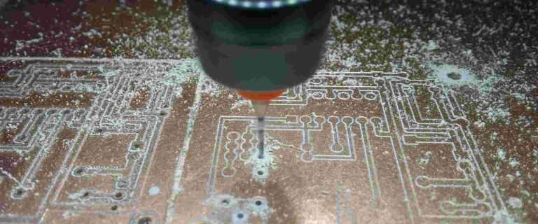
The first step in the SMD PCB assembly process is the application of solder paste.
Solder paste, a mixture of powdered solder and flux, is applied to the PCB using a stencil. The stencil, which is a thin metal sheet with openings corresponding to the pads on the PCB, ensures that the solder paste is deposited accurately and consistently. This step is critical because the amount and placement of solder paste directly affect the quality of the solder joints.
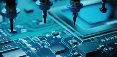
Following the application of solder paste, the next step is the placement of SMD components.
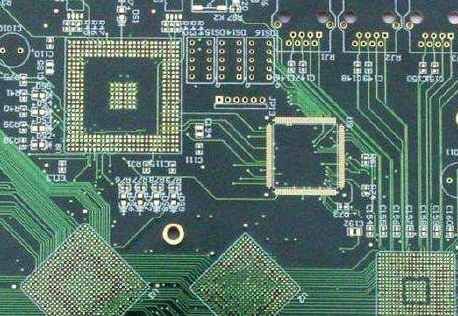
This is typically done using automated pick-and-place machines, which are capable of placing components with high precision and speed. These machines use a combination of vision systems and vacuum nozzles to pick up components from reels or trays and place them onto the PCB. The accuracy of this step is vital, as even slight misalignments can lead to defects or failures in the final product.
Once the components are placed, the assembly moves to the reflow soldering stage.
During reflow soldering, the PCB is passed through a reflow oven, where it is subjected to controlled heating and cooling cycles. The heat causes the solder paste to melt and form solid solder joints between the components and the PCB pads. The cooling phase then solidifies these joints, ensuring a strong and reliable connection. The temperature profile of the reflow oven must be carefully controlled to prevent damage to the components and ensure proper soldering.
After reflow soldering, the assembled PCB undergoes inspection and testing.
Automated optical inspection (AOI) systems are commonly used to check for defects such as solder bridges, missing components, and misalignments. AOI systems use cameras and image processing software to compare the assembled PCB against a reference model, identifying any discrepancies. In addition to AOI, X-ray inspection may be used to examine solder joints that are not visible, such as those under ball grid array (BGA) components. Electrical testing, including in-circuit testing (ICT) and functional testing, is also performed to verify that the PCB operates as intended.
If any defects are detected during inspection and testing, rework and repair processes are initiated.
Skilled technicians use specialized tools to remove and replace defective components, ensuring that the final product meets quality standards. This step is essential for maintaining the reliability and performance of the assembled PCB.
Finally, the assembled and tested PCBs are cleaned to remove any residual flux and contaminants.
Cleaning is typically done using solvents or ultrasonic cleaning systems, depending on the type of flux used and the specific requirements of the assembly. Cleanliness is important to prevent corrosion and ensure the long-term reliability of the PCB.
In conclusion, the SMD PCB assembly process involves several key steps, each of which plays a crucial role in ensuring the quality and functionality of the final product. From solder paste application and component placement to reflow soldering, inspection, and cleaning, each step must be executed with precision and care. Understanding these steps and their importance is essential for anyone involved in electronics manufacturing.
Common Challenges In SMD PCB Assembly And How To Overcome Them
Surface Mount Device (SMD) PCB assembly is a critical process in modern electronics manufacturing, offering numerous advantages such as reduced size, improved performance, and cost efficiency. However, it also presents several challenges that can impact the quality and reliability of the final product. Understanding these common challenges and implementing effective strategies to overcome them is essential for achieving optimal results in SMD PCB assembly.
One of the primary challenges in SMD PCB assembly is component placement accuracy.
As electronic devices become increasingly compact, the components used in SMD assembly are correspondingly smaller. This miniaturization necessitates precise placement to ensure proper functionality and to avoid issues such as short circuits or open circuits. To address this challenge, manufacturers can employ advanced pick-and-place machines equipped with high-resolution cameras and sophisticated algorithms. These machines can accurately position components on the PCB, significantly reducing the risk of placement errors.
Another significant challenge is solder paste application.
Solder paste is a critical material in SMD assembly, serving as the adhesive that holds components in place and provides the electrical connection between the components and the PCB. Inconsistent or insufficient solder paste application can lead to defects such as solder bridges, tombstoning, or insufficient solder joints. To mitigate this issue, manufacturers can utilize automated stencil printers that ensure uniform and precise application of solder paste. Additionally, regular maintenance and calibration of the stencil printer can help maintain consistent performance.
Thermal management is also a crucial aspect of SMD PCB assembly.
During the reflow soldering process, the PCB and its components are subjected to high temperatures to melt the solder paste and form reliable solder joints. However, improper thermal profiles can result in defects such as solder voids, component warping, or thermal stress. To overcome this challenge, manufacturers should carefully design and control the reflow oven’s thermal profile, ensuring that it is tailored to the specific requirements of the components and the PCB. This can be achieved through thorough testing and optimization of the reflow process.
Component handling and storage present additional challenges in SMD PCB assembly.
Many SMD components are sensitive to moisture and electrostatic discharge (ESD), which can compromise their performance and reliability. To address these concerns, manufacturers should implement strict handling and storage protocols. This includes using moisture barrier bags, desiccant packs, and ESD-safe containers to protect components from environmental factors. Furthermore, personnel involved in the assembly process should be trained in proper handling techniques to minimize the risk of damage.
Inspection and quality control are vital to ensuring the success of SMD PCB assembly.
Despite the use of advanced machinery and processes, defects can still occur. Automated optical inspection (AOI) and X-ray inspection systems can be employed to detect and identify defects such as misaligned components, solder joint issues, or hidden voids. These inspection systems provide valuable feedback, allowing manufacturers to identify and rectify problems early in the assembly process, thereby improving overall yield and reliability.
In conclusion, while SMD PCB assembly offers numerous benefits, it also presents several challenges that must be addressed to ensure high-quality and reliable electronic products. By leveraging advanced machinery, implementing stringent process controls, and employing thorough inspection techniques, manufacturers can effectively overcome these challenges. This approach not only enhances the efficiency and accuracy of the assembly process but also contributes to the production of robust and reliable electronic devices.
Innovations In SMD PCB Assembly Technology
Surface Mount Device (SMD) PCB assembly has undergone significant advancements in recent years, driven by the relentless pursuit of miniaturization, efficiency, and reliability in electronic devices. These innovations have not only enhanced the performance of electronic products but also streamlined the manufacturing process, making it more cost-effective and environmentally friendly.
One of the most notable advancements in SMD PCB assembly technology is the development of high-precision placement machines.
These machines are capable of placing components with remarkable accuracy, often within micrometers. This precision is crucial as electronic devices continue to shrink in size, necessitating the placement of increasingly smaller components on densely packed PCBs. The use of advanced vision systems and machine learning algorithms has further improved the accuracy and speed of these placement machines, reducing the likelihood of errors and increasing overall production efficiency.
In addition to placement accuracy, the soldering process has also seen significant improvements.
Traditional wave soldering methods have largely been replaced by reflow soldering techniques, which offer better control over the soldering process and result in higher quality joints. Reflow soldering involves the application of solder paste to the PCB, followed by the placement of components and the application of heat to melt the solder, creating strong and reliable connections. Innovations in solder paste formulations and reflow oven technology have further enhanced the reliability and performance of solder joints, reducing the risk of defects such as voids and cold solder joints.
Another key innovation in SMD PCB assembly is the adoption of automated optical inspection (AOI) systems.
These systems use high-resolution cameras and sophisticated image processing algorithms to inspect PCBs for defects such as misaligned components, solder bridges, and insufficient solder. By identifying defects early in the production process, AOI systems help to reduce the number of defective products that reach the end of the production line, thereby improving overall product quality and reducing waste. Furthermore, the integration of AOI systems with other manufacturing processes allows for real-time feedback and adjustments, further enhancing production efficiency.
The use of advanced materials has also played a significant role in the evolution of SMD PCB assembly technology.
High-performance substrates, such as those made from polyimide or ceramic, offer superior thermal and electrical properties compared to traditional FR4 materials. These advanced substrates enable the production of PCBs that can withstand higher operating temperatures and offer better signal integrity, making them ideal for use in high-performance applications such as aerospace, automotive, and telecommunications. Additionally, the development of lead-free solder alloys has addressed environmental concerns associated with traditional lead-based solders, making the manufacturing process more sustainable.
Moreover, the advent of Industry 4.0 and the Internet of Things (IoT) has brought about a new era of smart manufacturing in SMD PCB assembly.
The implementation of interconnected machines and data analytics allows for greater visibility and control over the production process. Real-time monitoring and predictive maintenance can identify potential issues before they lead to costly downtime, while data-driven decision-making can optimize production schedules and resource allocation. This level of automation and connectivity not only enhances production efficiency but also enables manufacturers to respond more quickly to changes in demand and market conditions.
In conclusion, the innovations in SMD PCB assembly technology have significantly transformed the electronics manufacturing landscape. High-precision placement machines, advanced soldering techniques, automated optical inspection systems, the use of advanced materials, and the integration of smart manufacturing practices have collectively contributed to the production of smaller, more reliable, and higher-performing electronic devices. As technology continues to evolve, it is likely that further advancements will continue to drive improvements in SMD PCB assembly, ensuring that the electronics industry can meet the ever-increasing demands of consumers and businesses alike.