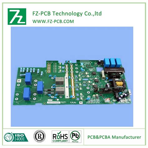
SMT board assembly – Get free custom quote
SMT PCB
What is SMT?
Surface Mount Technology (SMT) is a new generation of electronic assembly technology. It compresses traditional electronic components into devices with a volume of only a few tens of times smaller, thus achieving high density, high reliability, miniaturization, low cost, and automated production of electronic product assembly. This miniaturized component is called SMY device (or SMC, chip device). The process of assembling components on a printed (or other substrate) substrate is called SMT process. The related assembly equipment is called SMT equipment.
At present, advanced electronic products, especially computer and communication electronic products, have widely adopted SMT technology. The output of SMD devices in the world has increased year by year, while the output of traditional devices has decreased year by year. Therefore, with the passage of time, SMT technology will become more and more popular.
In other words, SMT is the abbreviation of Surface Mounted Technology, which is the most popular technology and process in the current electronic assembly industry.

What are the characteristics of SMT:
High assembly density, small size and light weight of electronic products. The size and weight of patch components are only about 1/10 of traditional plug-in components. Generally, after using SMT, the size of electronic products is reduced by 40%~60%, and the weight is reduced by 60%~80%.
High reliability and strong vibration resistance. Low solder joint defect rate.
Good high-frequency characteristics. Reduced electromagnetic and radio frequency interference.
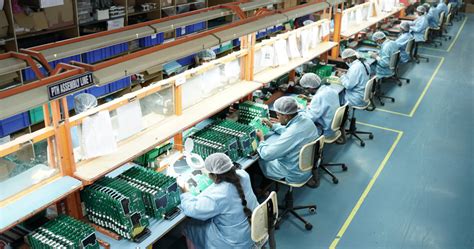
Easy to realize automation and improve production efficiency. Reduce costs by 30%~50%. Save materials, energy, equipment, manpower, time, etc.
GET PCB MANUFACTURING AND ASSEMBLY QUOTE NOW!
Why use SMT:
Electronic products pursue miniaturization, and the perforated plug-in components used before can no longer be reduced.
Electronic products have more complete functions, and the integrated circuits (ICs) used no longer have perforated components, especially large-scale and highly integrated ICs. Surface mount components have to be mass-produced and automated. The factory must produce high-quality products at low cost and high output to meet customer needs and enhance market competitiveness. The development of electronic components, the development of integrated circuits (ICs), and the diversified application of semiconductor materials are imperative for the electronic technology revolution and pursue international trends.

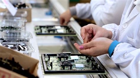
Basic SMT process components:
Screen printing (or dispensing), reflow soldering, mounting (curing), cleaning, testing, and rework.
Screen printing: Its function is to print solder paste or patch glue onto the pads of the PCB to prepare for the soldering of components. The equipment used is a screen printer (screen printer), which is located at the forefront of the SMT production line.
Dispensing: It is to drip glue onto a fixed position of the PCB. Its main function is to fix components to the PCB board. The equipment used is a dispensing machine, which is located at the forefront of the SMT production line or behind the testing equipment.
Reflow soldering: Its function is to melt the solder paste so that the surface mounted components and the PCB board are firmly bonded together. The equipment used is a reflow oven, which is located behind the mounter in the SMT production line.
Mounting: Its function is to accurately install the surface mounted components on the fixed position of the PCB. The equipment used is a mounter, which is located behind the screen printer in the SMT production line.
Curing: Its function is to melt the patch glue so that the surface mounted components and PCB boards are firmly bonded together. The equipment used is a curing furnace, which is located behind the SMT production line.
Cleaning: Its function is to remove the soldering residues such as flux that are harmful to the human body on the assembled PCB board. The equipment used is a cleaning machine, which can be in a non-fixed position and can be online or offline.
Detection: Its function is to detect the welding quality and assembly quality of the assembled PCB board. The equipment used includes magnifying glasses, microscopes, online testers (ICT), flying probe testers, automatic optical inspection (AOI), X-RAY inspection systems, functional testers, etc. The position can be configured in a suitable place on the production line according to the needs of the inspection.
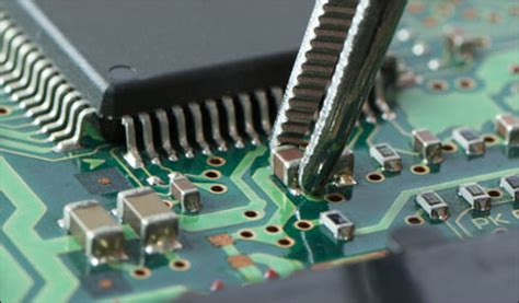
Rework: Its function is to rework the PCB board that has a fault in the inspection. The tools used are soldering irons, rework workstations, etc. Configured at any position in the production line.
GET PCB AND ASSEMBLY SERVICE QUOTE NOW!
Common knowledge of SMT
1. Generally speaking, the temperature specified in the SMT workshop is 25±3℃.
2. When printing solder paste, the materials and tools required are solder paste, steel plate, scraper, wiping paper, dust-free paper, cleaning agent, and stirring knife.
3. The commonly used solder paste alloy composition is Sn/Pb alloy, and the alloy ratio is 63/37.
4. The main components of solder paste are divided into two parts: tin powder and flux.
5. The main function of flux in welding is to remove oxides, destroy the surface tension of molten tin, and prevent re-oxidation.
6. The volume ratio of tin powder particles to Flux (flux) in solder paste is about 1:1, and the weight ratio is about 9:1.
7. The principle of taking solder paste is first in, first out.
8. When solder paste is opened and used, it must go through two important processes: temperature return and stirring.
9. Common methods for making steel plates are: etching, laser, and electroforming.
10. The full name of SMT is Surface mount (or mounting) technology, which means surface adhesion (or mounting) technology in Chinese.
11. The full name of ESD is Electro-static discharge, which means electrostatic discharge in Chinese.
12. When making SMT equipment programs, the program includes five parts, which are PCB data; Mark data; Feeder data; Nozzle data; Part data.
13. The melting point of lead-free solder Sn/Ag/Cu 96.5/3.0/0.5 is 217C.
14. The controlled relative temperature and humidity of the parts drying oven is < 10%.
15. Commonly used passive components (Passive Devices) include: resistors, capacitors, point sensors (or diodes), etc.; active components (Active Devices) include: transistors, ICs, etc.
16. The material of the commonly used SMT steel plate is stainless steel.
17. The thickness of the commonly used SMT steel plate is 0.15mm (or 0.12mm).
18. The types of electrostatic charge generation include friction, separation, induction, electrostatic conduction, etc.; the impact of electrostatic charge on the electronics industry is: ESD failure, electrostatic pollution; the three principles of static elimination are electrostatic neutralization, grounding, and shielding.
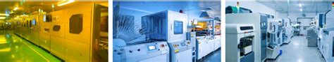
Introduction to SMT production line
The basic integrated SMT production line should contain a loader, printer, chip mounter, reflow oven, and unloader. The PCB starts from the loader, conveys along the path and passes through the equipment until the production is completed. Then, the PCB will receive high-temperature soldering through the reflow oven and be conveyed to the unloader after the printing, mounting, and soldering are completed.
PCB design elements that affect SMT manufacturing
PCB design is a key link in SMT technology, and SMT technology is an important factor in determining the quality of SMT manufacturing. This article will analyze the PCB design elements that affect its quality from the perspective of SMT equipment manufacturing. The design requirements of SMT manufacturing equipment for PCB mainly include: PCB pattern, size, positioning holes, clamping edges, MARK, panel routing, etc.
(1) PCB pattern
In the automatic SMT production line, PCB production starts from the loader and completes production after printing, chip mounting, and welding. Finally, it will be generated by the unloader as a finished board. In this process, the PCB is transmitted on the path of the equipment, which requires that the PCB pattern should be consistent with the path transmission between the equipment.
(2) PCB size
The PCB design size must meet the maximum and minimum size requirements of the placement machine. So far, the size of most equipment is in the range of 50mmx50mm to 330mmx250mm (or 410mmx360mm.
If the thickness of the PCB is too thin, its design size should not be too large. Otherwise, the reflow temperature will cause PCB deformation. The ideal aspect ratio is 3:2 or 4:3.
If the PCB size is smaller than the minimum size requirement of the equipment, it should be panelized. The number of panels depends on the size and thickness of the PCB.
(3) PCB positioning holes
SMT positioning methods are divided into two types: positioning holes and edge positioning and edge positioning. However, the most commonly used positioning method is Mark point alignment.
(4) PCB edge pressing
Since the PCB is transported on the path of the device, the components must not be placed in the direction of the clamping edge, otherwise the components will be squeezed by the device, affecting the installation of the chip. some components are placed near the lower edge of the PCB, so the upper and lower edges cannot be considered as clamping edges.
However, there are no components near the two side edges, so the two short edges can be used as clamping edges,
PCB design is a complex technology that must consider device requirements and component layout, pad design, and circuit design at the same time. Excellent PCB design is an important factor in ensuring product quality.
This article brings some issues that should be considered in PCB design from the perspective of SMT manufacturing. As long as enough attention is paid to these issues, fully automatic SMT manufacturing of SMT devices can be carried out.