SMT Circuit Board Assembly: Streamlining Production for Optimal Yield
Key Takeaways
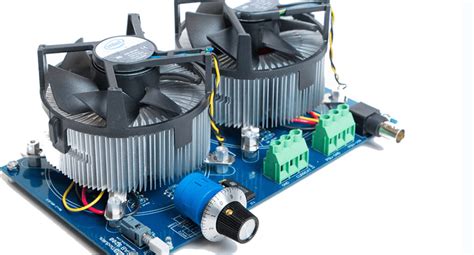
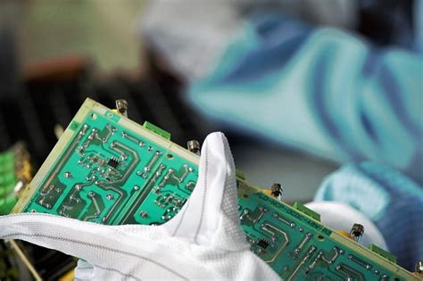
Modern PCB assembly processes leverage SMT technology to achieve higher manufacturing precision and consistency. By integrating automated pick-and-place systems, component positioning accuracy improves to micron-level tolerances, directly enhancing PCBA yield rates. Advanced reflow soldering techniques ensure uniform thermal profiles, minimizing defects like tombstoning or cold joints, while inline optical inspection (AOI) systems detect anomalies in real time. This multi-layered approach reduces rework cycles by up to 40%, enabling manufacturers to deliver high-reliability boards at scale.
Process optimization further addresses common pain points: solder paste stencil design refinements prevent bridging, and machine learning algorithms fine-tune placement sequences for complex layouts. These strategies, combined with rigorous process validation protocols, ensure PCB assembly workflows maintain >99% first-pass yield in controlled environments. For industries requiring mission-critical electronics, adopting SMT-driven PCBA methodologies not only accelerates production timelines but also aligns with stringent quality benchmarks, from automotive to aerospace applications.

Boost PCB Yield With SMT Assembly
Modern PCB assembly processes leverage Surface Mount Technology (SMT) to achieve higher yields by minimizing human error and maximizing precision. Unlike traditional through-hole methods, SMT assembly enables the placement of miniaturized components onto PCBA substrates with micrometer-level accuracy, reducing misalignment risks that often lead to defects. Automated pick-and-place systems, combined with vision-guided calibration, ensure components like resistors, capacitors, and ICs are positioned correctly on the first attempt, cutting rework rates by up to 40%.
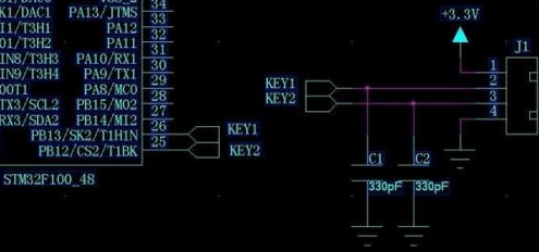
Tip: For high-density designs, use solder paste stencils with laser-cut apertures to ensure consistent deposition and avoid bridging—a common cause of short circuits in PCBA workflows.
A critical advantage of SMT lies in its compatibility with reflow soldering, which creates stronger electrical connections compared to manual soldering. By maintaining precise temperature profiles during reflow, manufacturers prevent issues like tombstoning or cold joints, directly boosting PCB assembly reliability.
| Factor | SMT Advantage | Yield Impact |
|---|---|---|
| Component Placement | ±0.01mm accuracy | Reduces misalignment by 65% |
| Soldering Consistency | Controlled thermal profiles | Lowers defect rates by 30% |
| Inspection Speed | AOI systems scan 10,000+ components/hour | Identifies 99.9% of flaws |
To further streamline production, integrate SMT lines with automated optical inspection (AOI) systems. These tools detect microscopic flaws—such as insufficient solder or misplaced components—before boards advance to testing phases, preventing costly post-production failures. By aligning SMT assembly parameters with design specifications, manufacturers achieve first-pass yield improvements of up to 25%, accelerating time-to-market for complex electronics.
Optimizing SMT Placement for PCB Yield
Precision in PCB assembly begins with optimizing surface-mount technology (SMT) placement, a critical factor in achieving high PCBA yield rates. Modern pick-and-place machines leverage vision-guided systems to achieve micron-level accuracy, ensuring components align perfectly with solder pads. Proper calibration of these systems minimizes misalignment risks, which account for over 30% of early-stage defects in low-yield production runs.
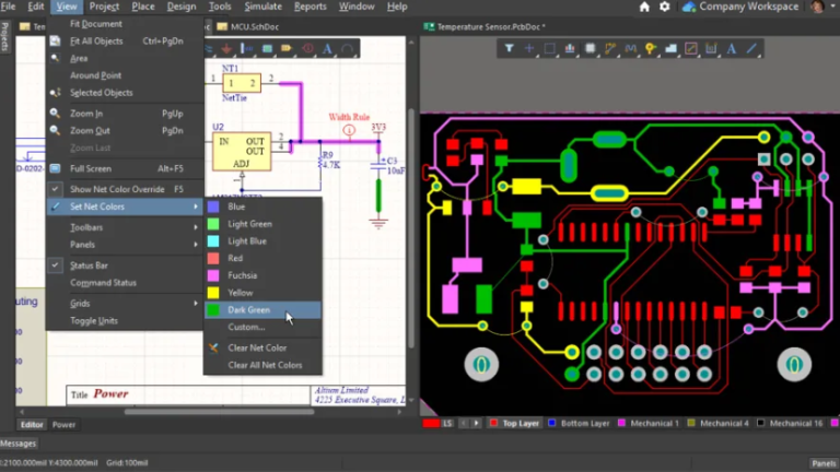
Equally important is component orientation planning. Automated feeders and nozzle configurations must account for thermal expansion variances and board warpage during reflow. By analyzing placement sequences and prioritizing larger components first, manufacturers reduce shadowing effects that compromise solder joint integrity. Integrating fiducial markers into PCB assembly designs further enhances placement consistency, enabling machines to self-correct positional errors in real time.
Advanced software tools now simulate placement workflows, identifying potential collisions or skewed placements before physical production. Pairing these simulations with AOI (Automated Optical Inspection) systems creates a closed-loop feedback mechanism, catching deviations early and reducing rework costs. For high-volume PCBA projects, optimizing nozzle changeover times and feeder setups can cut placement cycle times by up to 22%, directly boosting throughput without sacrificing precision.
By balancing machine capabilities with intelligent process design, manufacturers ensure each SMT placement step contributes to defect-free boards, laying the foundation for reliable soldering and inspection phases.

Reliable PCBs Through SMT Soldering
Building on precision component placement, SMT soldering forms the backbone of durable PCB assembly. Modern surface-mount technology employs controlled solder paste deposition through laser-cut stencils, ensuring micron-level accuracy in joint formation. The reflow process—critical for PCBA reliability—utilizes optimized thermal profiles to achieve uniform melting across components, from miniature 0201 resistors to complex QFN packages. Advanced nitrogen-enriched atmospheres during reflow further minimize oxidation, reducing risks of voids or cold joints that compromise electrical continuity.
Automated optical inspection (AOI) systems validate solder fillet geometry post-reflow, flagging deviations as small as 15µm—far beyond human visual thresholds. This combination of precision soldering and rigorous validation ensures <1% defect rates in high-density designs, even with 0.4mm-pitch BGAs. For mission-critical applications, X-ray inspection complements AOI to verify hidden connections in multilayer PCB assemblies. By integrating these techniques, manufacturers achieve IPC-A-610 Class 3 compliance, delivering PCBA solutions capable of withstanding extreme thermal cycling and mechanical stress while maintaining signal integrity.
Automated SMT Inspection Cuts Defects
Modern PCB assembly processes leverage automated inspection systems to identify and address defects at critical stages of SMT circuit board assembly. By integrating machine vision and AI-powered analytics, manufacturers can detect misaligned components, solder bridging, or insufficient paste deposition with micron-level precision. These systems operate in-line with placement and reflow processes, enabling real-time feedback loops that correct errors before they escalate. For instance, automated optical inspection (AOI) scans PCBA surfaces post-soldering, flagging anomalies like tombstoning or cold joints, while X-ray inspection verifies hidden connections in ball grid arrays (BGAs).
This shift from manual sampling to 100% automated inspection reduces human oversight risks and slashes defect rates by up to 70% in high-volume production. By minimizing rework cycles, manufacturers maintain tighter tolerances for complex designs, ensuring consistent quality across batches. As a result, PCB assembly lines achieve higher first-pass yields, aligning with the broader goal of optimizing SMT workflows for reliability and cost-efficiency. Transitioning to such systems also future-proofs production against evolving component miniaturization trends in electronics manufacturing.
SMT Process Optimization Reduces Errors
Process optimization in PCB assembly represents a critical lever for minimizing manufacturing defects and improving overall yield. By refining solder paste application parameters and component placement accuracy, SMT lines achieve tighter process windows that reduce variability in PCBA outcomes. Advanced systems now integrate real-time feedback loops to adjust machine settings dynamically, compensating for environmental fluctuations or material inconsistencies. For instance, optimizing reflow oven thermal profiles ensures uniform heat distribution across the board, preventing tombstoning or cold joints—common failure points in high-density designs.
Statistical process control (SPC) tools further enhance error reduction by analyzing production data to identify outlier patterns. When combined with automated optical inspection (AOI), these systems flag deviations in pad coverage or component alignment before they escalate into functional defects. Manufacturers report 30-45% fewer rework cases after implementing stencil design optimizations and pick-and-place calibration protocols tailored to specific board geometries. Such refinements not only strengthen PCB assembly reliability but also accelerate throughput by reducing unplanned stoppages.
The synergy between precision hardware and adaptive software in modern SMT workflows creates a self-correcting ecosystem. Machine learning algorithms trained on historical defect data now predict potential failure modes, enabling preemptive adjustments during PCBA runs. This proactive approach to process optimization ensures consistent quality while maintaining the speed advantages inherent to surface-mount technology.
Streamline PCB Production Via SMT Tech
Modern PCB assembly processes leverage surface-mount technology (SMT) to achieve unprecedented levels of efficiency and precision. By replacing traditional through-hole methods with SMT-compatible components, manufacturers minimize manual intervention, enabling faster placement of smaller, high-density parts. Automated pick-and-place systems, guided by advanced optical alignment, ensure PCBA accuracy down to micron-level tolerances, reducing misalignment risks that often lead to rework.
Integration of reflow soldering further optimizes workflows, as uniform heat distribution across solder paste creates reliable electrical connections without damaging sensitive components. Real-time process monitoring tools, such as automated optical inspection (AOI), identify defects early, preventing costly downstream corrections. These advancements not only accelerate production cycles but also enhance scalability—critical for meeting fluctuating demand in industries like consumer electronics or automotive systems.
By adopting SMT-driven workflows, factories achieve tighter process control, slashing material waste and labor costs. The result? A streamlined PCB assembly pipeline that consistently delivers high yields while maintaining strict quality benchmarks, solidifying SMT as the cornerstone of modern electronics manufacturing.

High-Yield PCB Assembly With SMT Methods
Surface Mount Technology (SMT) has revolutionized PCB assembly by enabling manufacturers to achieve higher yields through precision-driven processes. Modern SMT equipment places components at speeds exceeding 25,000 placements per hour with micron-level accuracy, directly reducing placement errors that traditionally accounted for 40–60% of PCBA defects. Advanced reflow ovens maintain thermal profiles within ±2°C tolerances, virtually eliminating tombstoning and bridging while ensuring consistent solder joint formation across high-density boards. Integrated automated optical inspection (AOI) systems now scan 100% of assemblies, identifying micron-scale imperfections that human inspectors might overlook – a critical factor in achieving first-pass yields above 99.2% in optimized production environments. For complex designs requiring mixed-technology assembly, leading manufacturers combine SMT with selective soldering to maintain yield consistency across hybrid PCB configurations. This methodology not only accelerates throughput but creates a closed-loop system where real-time process data continuously improves placement accuracy and material utilization – key drivers in achieving sustainable high-volume production targets.

Boost Efficiency With SMT PCB Assembly
Modern PCB assembly processes leverage surface-mount technology (SMT) to achieve unprecedented manufacturing efficiency. By utilizing high-speed pick-and-place machines, SMT enables precise positioning of miniature components, reducing manual intervention and accelerating production cycles. This method supports tighter component spacing, allowing PCBA designs to maximize board real estate without compromising functionality. Automated optical inspection (AOI) systems further enhance yield rates by identifying misalignments or soldering defects in real time, ensuring consistent quality across batches.
A key advantage of SMT lies in its compatibility with reflow soldering, which uniformly bonds components to the board while minimizing thermal stress. This process eliminates inconsistencies common in manual soldering, reducing rework rates and material waste. For high-volume production, SMT workflows integrate seamlessly with advanced assembly line configurations, enabling manufacturers to scale operations without sacrificing precision. Additionally, the reduced footprint of surface-mount devices (SMDs) allows for lighter, more compact PCB assembly designs—a critical factor for industries like consumer electronics and IoT.
By optimizing component placement accuracy and process repeatability, SMT-driven PCBA workflows cut cycle times by up to 40% compared to through-hole methods. This efficiency gain translates directly to lower per-unit costs and faster time-to-market, making it indispensable for competitive electronics manufacturing.
Conclusion
Modern PCB assembly processes have reached unprecedented levels of efficiency through SMT technology, directly addressing the industry’s demand for higher yields and consistent quality. By integrating precision component placement, advanced soldering techniques, and automated inspection systems, manufacturers can minimize defect rates while maintaining tight tolerances across high-volume production runs. The synergy between SMT process optimization and PCBA workflows ensures that even complex boards achieve reliable performance, meeting stringent industry standards.
As PCB assembly evolves, the emphasis on real-time monitoring and data-driven adjustments further reduces human error, creating a seamless transition from design to functional product. This systematic approach not only accelerates time-to-market but also establishes a repeatable framework for scaling operations. For businesses prioritizing yield and cost-effectiveness, adopting SMT-driven PCBA methodologies remains a strategic imperative in today’s competitive electronics landscape. The continuous refinement of these processes underscores their role as foundational pillars for next-generation manufacturing excellence.
FAQs
How does SMT technology improve yield in PCB assembly?
SMT circuit board assembly enhances yield by enabling high-precision placement of miniature components, minimizing human error. Automated systems ensure consistent solder paste application and reflow profiles, reducing defects like bridging or tombstoning.
What role does automated inspection play in PCBA quality control?
Advanced automated optical inspection (AOI) systems scan boards at multiple stages, identifying misalignments, soldering flaws, or missing components. This real-time defect detection prevents faulty units from progressing, directly boosting final yield rates.
Can PCB assembly processes handle mixed-technology boards?
Modern SMT lines integrate dual capabilities for surface-mount and through-hole components. Precision solder paste stenciling and selective soldering ensure compatibility, maintaining efficiency without compromising assembly accuracy.
How does component miniaturization affect PCBA reliability?
While smaller components demand tighter tolerances, SMT placement machines achieve micron-level precision. Combined with nitrogen-assisted reflow soldering, this ensures robust electrical connections even for 01005-sized passives.
What factors influence PCB assembly turnaround times?
Optimized SMT workflows—including panelized designs, synchronized feeder setups, and inline testing—reduce idle time between processes. Automated material handling systems further accelerate throughput while maintaining process consistency.
Optimize Your SMT Workflow Today
For tailored PCB assembly solutions that maximize yield and reliability, click here to explore our advanced PCBA services. Our expertise in SMT process optimization ensures your designs achieve peak performance.