Solutions to PCB manufacturing process defects
There are many processes involved in the PCB manufacturing process, and quality defects may occur in each process. These quality problems always involve many aspects and are difficult to solve. The causes of the problems are multifaceted, some of which are related to chemistry, mechanics, plates, optics, etc. After decades of production practice, combined with the actual experience of solving quality problems and relevant information on solving technical problems, the following is a summary:
Defects, causes and solutions in PCB manufacturing process
Process Defects Causes Solutions
Filming The film layer on the board has bubbles The board surface is not clean Check the wettability of the board surface, that is, the clean surface can maintain water uniformity and continuous water film for up to 1 minute
Filming temperature and pressure are too low Increase temperature and pressure
The edge of the film layer is warped Due to excessive tension in the film layer, the film layer has poor adhesion Adjust the pressure screw
Film layer shrinkage The film layer has poor contact with the board surface Tighten the pressure screw
Exposure Poor resolution Due to scattered light and reflected light reaching the film layer cover Reduce exposure time
Overexposure Reduce exposure time
Image yin and yang difference; sensitivity is too low Make the minimum yin and yang difference ratio 3:1
Film has poor contact with the board surface Check the vacuum system
After adjustment, the light intensity is insufficient Adjust again
Overheating Check the cooling system
Intermittent exposure Continuous exposure
Poor storage conditions for dry film Working under light
Development There is scum on the developing area Insufficient development, resulting in colorless film remaining on the board surface Slow down and increase the development time
Developer composition is too low Adjust the content to reach 1.5-2% sodium carbonate
Developer contains too much film quality Replace
Development and cleaning interval is too long Not more than 10 minutes
Developer injection pressure is insufficient Clean the filter and check the nozzle
Overexposure Correct the exposure time
Improper sensitivity The ratio of maximum to minimum sensitivity shall not be less than 3
Film discoloration, surface is not bright Insufficient exposure, resulting in insufficient polymerization of the film layer Increase exposure and drying time
Overdevelopment Reduce the development time, correct the temperature and cooling system, and check the developer content
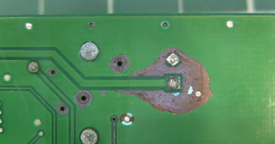
Film layer falls off the board surface Due to insufficient exposure or excessive development, the film layer is not firmly attached Increase exposure time, reduce development time and correct content
Surface is not clean Check the surface wettability
After the film is exposed, it is immediately developed. After the film is applied and exposed, it should be left for at least 15 to 30 minutes
There is excess glue on the circuit pattern. The dry film is expired. Replace it
Insufficient exposure. Increase the exposure time
The surface of the film is not clean. Check the quality of the film
The developer composition is improper. Make adjustments
The development speed is too fast. Make adjustments