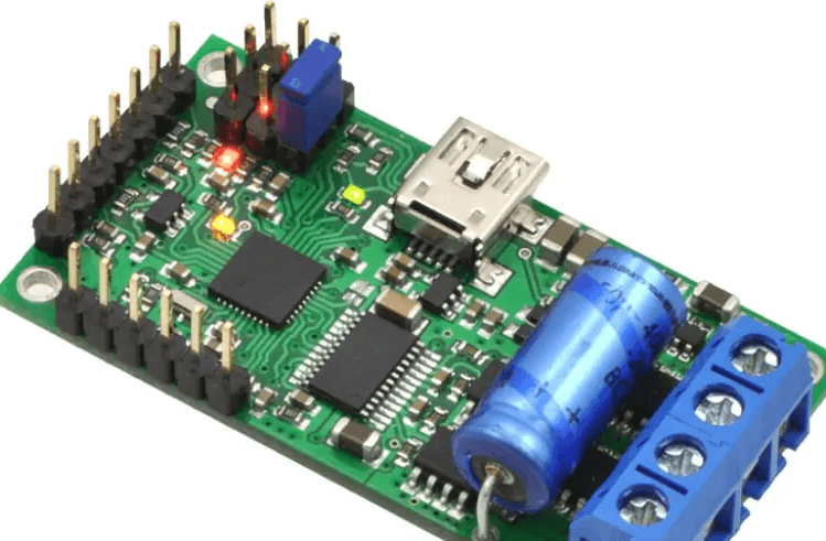
Some knowledge about pcb vias
PCB is an important electronic component and a support for electronic components. Without PCB, our electronic devices basically cannot operate. In order to enhance everyone’s understanding of PCB, this article will introduce the PCB through-hole size requirements, PCB through-hole types, and PCB through-hole filling procedures. If you are interested in PCB, you may wish to continue reading.
1.PCB through-hole size requirements
Printed circuit board (PCB) is hailed as the mother of electronic products by many people. It is a key component of consumer electronic products such as computers and mobile phones. It is widely used in medical, aviation, new energy, automobile and other industries. Almost every day we experience the convenience brought by electronic products. Looking at the brief history of PCB development, every technological advancement directly or indirectly affects all mankind. This shows the importance of PCB. In this part, let’s take a look at the PCB through-hole size requirements.
(1)PCB through-hole size
The size of PCB through-holes can vary depending on their location, purpose and other factors, which is why each PCB manufacturer provides several PCB drill bit sizes. Most manufacturers can make holes as small as 0.15 mm or larger holes of 1 mm or larger. When considering the size of the hole you want, you also need to consider the annular ring, or the copper pad surrounding the drill hole, that it will form.
How do you calculate the annular ring? The ideal annular ring is equal to the sum of the diameter of the copper pad minus the diameter of the drill hole divided by 2, which gives the drill the best chance of hitting the center of the pad for optimal connectivity.
(2)Standard via sizes
There aren’t necessarily any standard PCB via sizes in PCB manufacturing, as PCB standard via sizes tend to vary from manufacturer to manufacturer. However, many PCB manufacturers like to use commonly used drill sizes, which they may refer to as standard PCB drill sizes. One of the most common sizes is 0.6 mm, but 0.2 mm and 0.3 mm are also commonly used.
2.PCB via types
You can use each standard via size to create various types of PCB vias, depending on the layers, construction, design, and purpose of the PCB. The three most common types of PCB vias are:
(1)Plated through holes
Plated through holes (PTHs) are vias that run through all layers of a PCB to connect the top and bottom layers. You should be able to see the PTH from one end of the PCB to the other. PTHs can be either plated or non-plated. Non-plated through-holes are not conductive, while plated through-holes are plated, which means that they are conductive in all layers of the PCB.
(2)Blind vias
Blind vias connect the outer layer (top or bottom layer) of a PCB to one or more inner layers, but do not drill completely through the board. Accurate drilling of blind vias can be challenging, so blind vias are generally more expensive to manufacture than PTHs.
(3)Buried vias
Buried vias also increase the cost of PCBs because they are difficult to manufacture. This type of via is located in the inner layers of the PCB to connect two or more inner layers. You cannot see the buried vias on the outer layers of the PCB.
(4)Things to consider
In the process of creating a PCB, there are a few things to consider. First, you should understand what is the aspect ratio in PCB design. The aspect ratio is the thickness of the PCB relative to the diameter of the through-hole drill, and it determines the reliability of copper plating on the PCB. The higher the ratio, the more difficult it is to get reliable plating, which affects the type of vias and plating methods you choose.
Buried or blind vias may serve your PCB better with a 15:1 aspect ratio, while PTHs can work well with a low aspect ratio of 2:1. How do you choose the thickness of your PCB copper? Typically, vias in outer layers, such as through-holes, require a thicker copper layer than internal buried vias. The voltage used by the PCB also affects the copper thickness. High-voltage applications typically require thicker PCB copper than low-voltage applications.
3.via filling procedures
Sometimes it is necessary to fill PCB vias, such as to reduce the risk of trapped air or to increase conductivity. Some common methods for filling vias include:
(1)Via tenting
Via tenting creates a solder mask layer over the PCB via instead of filling the hole with material. This can be a quick, simple, and cost-effective option for covering vias, but tented vias may reopen over time.
(2)Via plugging
The via plugging process fills the hole with non-conductive material and seals it with a mask. Via plugging also covers the annular ring and does not produce a smooth, finished surface.
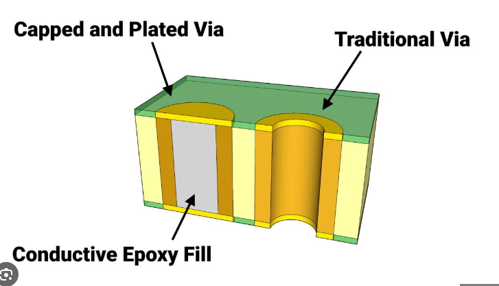
(3)Through-hole filling
Through-hole filling uses resin to create a permanently filled hole. Through-hole filling is a commonly used through-hole filling in which the manufacturer fills the through-hole with conductive material, plates the surface with copper, and then trims the surface. This process can route signals to other areas of the PCB.
4.Key points of pcb via setting
Different sizes of vias can be placed in a PCB due to the needs of different routings, but it is usually not recommended to exceed 3 types to avoid causing great inconvenience to production and increasing costs;
The depth to diameter ratio of the via is generally ≤6, because when it exceeds 6 times, it is difficult to ensure that the hole wall can be evenly copper plated;
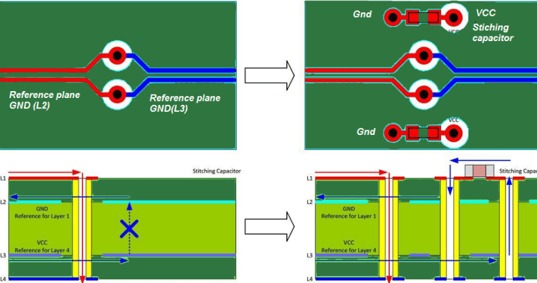
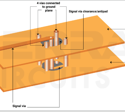
The parasitic inductance and parasitic capacitance of the via also need to be paid attention to, especially in high-speed circuits, special attention should be paid to its distributed performance parameters;
The smaller the via, the smaller the distributed parameters, the more suitable it is for high-speed circuits, but its cost is also high.
5.Methods for designing vias in multi-layer pcbs
The importance of via technology in PCB design cannot be underestimated. Vias connect conductive materials of different layers to achieve signal transmission and power supply. The smoothness and quality of vias are crucial to the stability and reliability of the entire circuit.
In multi-layer PCB design, vias are divided into two main types: blind vias and through vias. Blind vias only connect a few independent layers, while through vias connect all layers of the entire circuit board. When choosing the right type of via, factors such as the complexity of the circuit board, signal type, and bandwidth requirements need to be considered.
During the design process, it is crucial to select the appropriate via size and number. Too small an aperture may cause problems such as current instability, signal loss, and voltage drop, while too large an aperture may cause current overload and uneven distribution. When determining the number of vias, it is necessary to balance the performance requirements of the circuit board and the complexity of manufacturing.
Via design also needs to consider via filling materials. Common via filling materials include copper plating, thermosetting resin, polyimide, etc. The selection of filling materials should be based on the application environment and requirements of the circuit board.
In the actual manufacturing process, vias should meet certain manufacturing specifications and requirements. These specifications include: the location and spacing of vias must meet the design requirements, the copper plating of vias should reach a certain thickness and quality, the hole wall quality of vias should be good, etc. Strict compliance with these specifications can ensure the quality and stability of vias.
In multi-layer PCB design, the layout of vias is also very important. Reasonable via layout can optimize the performance and wiring effect of the circuit board. Generally speaking, the layout of vias should be distributed as evenly as possible to avoid too many vias gathering in certain areas, which will reduce the wiring effect and increase the risk of signal interference.
In order to optimize vias in multi-layer PCB design, design engineers should pay close attention to the development and practice of technology. Proficient via technology and manufacturing processes can greatly improve the performance and reliability of PCBs. In addition, the use of advanced PCB design software and tools can also help designers better implement complex via designs.
Through the in-depth understanding and reasonable application of via technology in multi-layer PCB design, design optimization can be achieved. Reasonable via design can improve the performance, reliability and manufacturing efficiency of circuit boards.