Speakers for pcb high frequency
Designing High-Frequency PCB Speakers for Optimal Performance
Designing high-frequency PCB speakers for optimal performance requires a meticulous approach, as the intricacies involved in high-frequency signal transmission demand precision and expertise.
The first step in this process is understanding the fundamental principles of high-frequency signals and their behavior on printed circuit boards (PCBs).
High-frequency signals, typically defined as those above 1 MHz, are susceptible to various forms of interference and signal degradation, which can significantly impact the performance of PCB speakers.
To begin with, the choice of materials for the PCB is crucial.
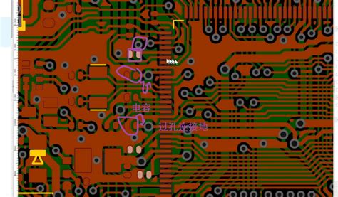
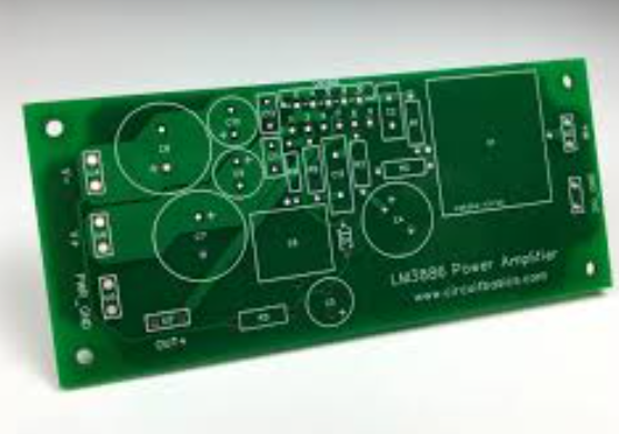
High-frequency applications often necessitate the use of low-loss dielectric materials, such as Rogers or Teflon, which exhibit minimal signal attenuation and maintain signal integrity over longer distances. These materials are preferred over standard FR-4 substrates, which may not provide the necessary performance characteristics for high-frequency operations. Additionally, the thickness of the PCB and the copper traces must be carefully considered to ensure minimal impedance and optimal signal transmission.
Another critical aspect is the layout and design of the PCB traces.
At high frequencies, the physical layout of the traces can significantly influence signal integrity. It is essential to maintain consistent trace widths and avoid sharp bends, as these can introduce reflections and signal loss. Utilizing microstrip or stripline configurations can help manage impedance and reduce electromagnetic interference (EMI). Furthermore, the use of ground planes and proper grounding techniques is vital to minimize noise and ensure a stable reference point for the signals.
Component selection also plays a pivotal role in the performance of high-frequency PCB speakers.
Passive components such as resistors, capacitors, and inductors must be chosen with care, considering their frequency response and parasitic elements. Surface-mount components are generally preferred over through-hole components due to their lower parasitic inductance and capacitance, which can adversely affect high-frequency performance. Additionally, active components such as amplifiers and transistors should be selected based on their frequency response and linearity to ensure accurate signal amplification and minimal distortion.
Thermal management is another important consideration in the design of high-frequency PCB speakers.
High-frequency signals can generate significant heat, which can affect the performance and reliability of the components. Effective thermal management strategies, such as the use of thermal vias, heat sinks, and proper airflow, are essential to dissipate heat and maintain optimal operating temperatures.
Moreover, signal integrity analysis and simulation tools are invaluable in the design process.
These tools allow designers to model and predict the behavior of high-frequency signals on the PCB, identify potential issues, and optimize the design before fabrication. Techniques such as time-domain reflectometry (TDR) and vector network analysis (VNA) can be employed to measure and analyze signal integrity, ensuring that the final design meets the desired performance specifications.
In conclusion, designing high-frequency PCB speakers for optimal performance involves a comprehensive understanding of high-frequency signal behavior, careful selection of materials and components, meticulous layout and design practices, effective thermal management, and the use of advanced simulation and analysis tools. By adhering to these principles, designers can create high-frequency PCB speakers that deliver superior performance, reliability, and sound quality.
Materials and Techniques for High-Frequency PCB Speaker Manufacturing
In the realm of high-frequency PCB speaker manufacturing, the selection of materials and techniques is paramount to achieving optimal performance and reliability. The intricate nature of high-frequency signals necessitates a meticulous approach to both the design and fabrication processes. This article delves into the critical materials and techniques that are employed to ensure the efficacy of high-frequency PCB speakers.
To begin with, the choice of substrate material is a fundamental consideration.
High-frequency applications demand substrates with low dielectric constants and minimal loss tangents to reduce signal attenuation and phase distortion. Materials such as Rogers RT/duroid, Taconic, and Arlon are frequently utilized due to their superior electrical properties. These substrates offer a stable dielectric constant over a wide frequency range, which is essential for maintaining signal integrity in high-frequency circuits.
In addition to substrate selection, the type of copper foil used in the PCB is equally important.
For high-frequency applications, rolled annealed (RA) copper is preferred over electro-deposited (ED) copper. RA copper has a smoother surface finish, which reduces signal loss and minimizes skin effect at high frequencies. The skin effect, where high-frequency currents tend to flow on the surface of conductors, can significantly impact the performance of PCB speakers if not properly managed.
Furthermore, the precision of the etching process plays a crucial role in high-frequency PCB manufacturing.
Advanced photolithography techniques are employed to achieve fine line widths and tight tolerances. This precision is necessary to ensure that the impedance of the transmission lines is controlled accurately, which is vital for maintaining signal fidelity. Any deviation in the line width or spacing can lead to impedance mismatches, resulting in signal reflections and loss.
Another critical aspect is the use of via structures in high-frequency PCBs.
Vias, which are used to connect different layers of the PCB, can introduce inductance and capacitance that affect signal performance. To mitigate these effects, techniques such as back-drilling are employed to remove the unused portion of the via, thereby reducing parasitic inductance. Additionally, the use of microvias, which are smaller in diameter than traditional vias, can help minimize signal degradation.
The solder mask material also warrants careful consideration.
In high-frequency applications, the solder mask can contribute to signal loss if its dielectric properties are not compatible with the substrate material. Low-loss solder masks are therefore used to ensure that the overall dielectric constant of the PCB remains consistent. This consistency is crucial for maintaining the integrity of high-frequency signals.
Moreover, the assembly process for high-frequency PCBs requires specialized techniques to ensure that the components are placed and soldered with high precision.
Surface mount technology (SMT) is commonly used, as it allows for the placement of components with minimal lead lengths, reducing inductive and capacitive effects. Additionally, the use of reflow soldering with controlled temperature profiles ensures that the components are securely attached without causing thermal damage to the sensitive high-frequency circuits.
In conclusion, the manufacturing of high-frequency PCB speakers involves a careful selection of materials and techniques to ensure optimal performance. From the choice of substrate and copper foil to the precision of the etching process and the management of via structures, each step is critical in maintaining signal integrity. By employing advanced materials and meticulous fabrication techniques, manufacturers can produce high-frequency PCB speakers that meet the stringent demands of modern electronic applications.
Troubleshooting Common Issues in High-Frequency PCB Speaker Systems
When dealing with high-frequency PCB speaker systems, troubleshooting common issues can be a complex yet essential task to ensure optimal performance.
One of the primary concerns in these systems is signal integrity, which can be compromised by various factors.
To begin with, impedance mismatches are a frequent culprit. These mismatches can cause signal reflections, leading to distortions and loss of signal quality. To mitigate this, it is crucial to ensure that the impedance of the transmission lines matches the impedance of the speaker and other components in the circuit. Utilizing proper impedance matching techniques, such as using matching networks or adjusting trace widths, can significantly improve signal integrity.
Another common issue is electromagnetic interference (EMI), which can severely affect the performance of high-frequency PCB speaker systems.
EMI can originate from various sources, including nearby electronic devices, power lines, and even the PCB layout itself. To address this, implementing proper shielding techniques is essential. This can involve using grounded metal enclosures or incorporating ground planes within the PCB design. Additionally, careful routing of high-frequency signals away from noisy components and minimizing loop areas can further reduce EMI susceptibility.
Thermal management is another critical aspect that cannot be overlooked.
High-frequency operations often generate significant heat, which can degrade the performance and reliability of the speaker system. Effective thermal management strategies include using heat sinks, thermal vias, and proper PCB materials with good thermal conductivity. Ensuring adequate ventilation and considering the thermal properties of components during the design phase can also help in maintaining optimal operating temperatures.
Component selection plays a pivotal role in the performance of high-frequency PCB speaker systems.
Using components with appropriate frequency ratings and low parasitic elements is essential. For instance, capacitors and inductors should be chosen based on their self-resonant frequencies to avoid unwanted resonances that can distort the signal. Additionally, selecting components with tight tolerances can help maintain consistent performance across different units.
The layout of the PCB itself is another area where issues can arise.
Poor layout practices can lead to crosstalk, signal degradation, and increased EMI. To avoid these problems, it is important to follow best practices for high-frequency PCB design. This includes maintaining short and direct signal paths, using differential signaling where possible, and ensuring proper grounding. Additionally, separating analog and digital grounds can help minimize noise coupling between different sections of the circuit.
Testing and validation are crucial steps in troubleshooting high-frequency PCB speaker systems.
Using tools such as network analyzers, oscilloscopes, and spectrum analyzers can help identify and diagnose issues related to signal integrity, EMI, and component performance. Performing thorough testing under various operating conditions can provide valuable insights into potential problems and their solutions.
In conclusion, troubleshooting common issues in high-frequency PCB speaker systems requires a comprehensive approach that addresses signal integrity, EMI, thermal management, component selection, PCB layout, and thorough testing. By understanding and mitigating these challenges, one can ensure the reliable and high-quality performance of high-frequency PCB speaker systems. This holistic approach not only enhances the system’s functionality but also extends its lifespan, ultimately leading to a more robust and efficient design.
Innovations in High-Frequency PCB Speaker Technology
The realm of high-frequency printed circuit board (PCB) speaker technology has witnessed significant advancements in recent years, driven by the demand for superior audio quality and the miniaturization of electronic devices. These innovations are not only enhancing the auditory experience but also pushing the boundaries of what is technically feasible in compact audio systems. As we delve into the intricacies of these developments, it becomes evident that the integration of high-frequency capabilities into PCB speakers is a multifaceted endeavor, involving a confluence of material science, engineering precision, and cutting-edge design methodologies.
To begin with, the materials used in the construction of high-frequency PCB speakers have undergone substantial refinement.
Traditional materials, while effective for lower frequency ranges, often fall short when tasked with handling the rapid oscillations required for high-frequency sound reproduction. Consequently, researchers have turned to advanced composites and specialized polymers that offer superior rigidity and reduced mass. These materials not only facilitate the rapid movement necessary for high-frequency sound waves but also minimize distortion, thereby ensuring a clearer and more accurate audio output.
In addition to material advancements, the design architecture of PCB speakers has seen remarkable innovation.
Modern high-frequency PCB speakers often employ micro-electromechanical systems (MEMS) technology, which allows for the creation of extremely small and precise components. MEMS technology enables the integration of intricate structures directly onto the PCB, thereby reducing the overall footprint of the speaker system. This miniaturization is particularly beneficial for applications in portable electronics, where space is at a premium. Moreover, MEMS-based designs can achieve higher resonant frequencies, making them ideal for high-frequency audio applications.
Furthermore, the implementation of advanced signal processing techniques has played a pivotal role in the evolution of high-frequency PCB speakers.
Digital signal processing (DSP) algorithms can be employed to enhance the performance of these speakers by compensating for any inherent limitations in the physical design. For instance, DSP can be used to equalize the frequency response, ensuring that the output remains consistent across the entire audible spectrum. Additionally, sophisticated filtering techniques can be applied to mitigate any unwanted noise or interference, thereby preserving the integrity of the high-frequency signals.
Another noteworthy development in this field is the advent of wireless communication technologies, which have revolutionized the way high-frequency PCB speakers are utilized. The integration of Bluetooth and Wi-Fi capabilities into these speakers has eliminated the need for cumbersome wiring, allowing for greater flexibility in device placement and usage. This wireless functionality is particularly advantageous in modern smart home systems, where seamless connectivity and ease of use are paramount.
Moreover, the focus on energy efficiency has led to the creation of high-frequency PCB speakers that consume significantly less power without compromising on performance. This is achieved through the use of low-power amplifiers and energy-efficient components, which not only extend the battery life of portable devices but also contribute to overall sustainability efforts.
In conclusion, the innovations in high-frequency PCB speaker technology are a testament to the relentless pursuit of excellence in the audio engineering domain. Through advancements in materials, design architecture, signal processing, wireless communication, and energy efficiency, these speakers are setting new standards for audio quality and functionality. As technology continues to evolve, it is anticipated that high-frequency PCB speakers will become even more integral to a wide array of applications, from consumer electronics to professional audio systems, thereby enriching the auditory experience for users around the globe.