Special Component PCB Layout Requirements: Key Considerations and Best Practices
Introduction
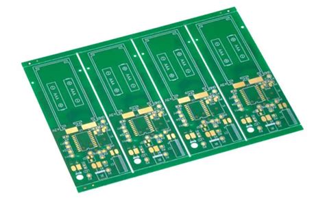
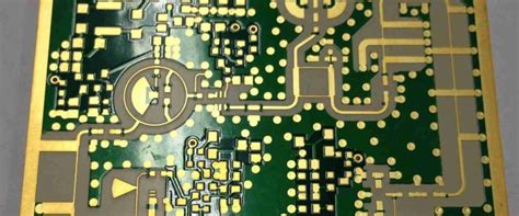
Printed Circuit Board (PCB) layout design is a critical phase in electronics development, directly impacting performance, reliability, and manufacturability. While standard components follow conventional design rules, special components—such as high-frequency devices, high-power modules, RF circuits, and precision analog components—require unique layout considerations. This article explores the essential requirements for PCB layout design involving special components, focusing on signal integrity, thermal management, electromagnetic compatibility (EMC), and manufacturability.
1. High-Frequency and RF Components
1.1 Impedance Matching and Controlled Routing
High-frequency signals, such as those in RF and microwave circuits, are highly sensitive to impedance mismatches. Proper trace width and dielectric spacing must be maintained to achieve the desired characteristic impedance (e.g., 50Ω or 75Ω). Key practices include:
- Use of Microstrip or Stripline Configurations: Microstrip traces (exposed on outer layers) and stripline traces (embedded between layers) help control impedance.
- Minimizing Vias: Each via introduces parasitic inductance and capacitance, which can degrade signal quality.
- Avoiding Sharp Bends: Right-angle bends cause impedance discontinuities; use curved or 45-degree traces instead.
1.2 Grounding and Shielding
- Continuous Ground Planes: A solid ground plane beneath high-frequency traces reduces loop inductance and crosstalk.
- Guard Rings and Shielding: Sensitive RF components should be surrounded by guard traces or shielding cans to prevent interference.
1.3 Isolation from Digital Noise
- Physical Separation: Keep high-frequency analog circuits away from high-speed digital signals to minimize coupling.
- Dedicated Power Planes: Use separate power supplies or filtering for RF and digital sections.

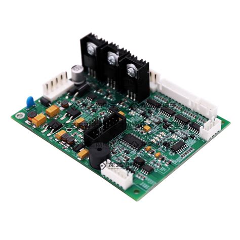
2. High-Power Components
2.1 Thermal Management
High-power components (e.g., power MOSFETs, voltage regulators) generate significant heat, requiring careful thermal design:
- Copper Pour and Thermal Reliefs: Use thick copper layers (2oz or more) for power traces and thermal vias to dissipate heat.
- Heatsinks and Thermal Pads: Directly attach heatsinks to components or use exposed pads (EPAD) for better heat transfer.
2.2 Current Handling and Trace Width
- Adequate Trace Sizing: Calculate trace widths based on current requirements (using IPC-2152 standards) to prevent overheating.
- Avoiding Neck-Down Regions: Ensure power traces maintain uniform width without sudden constrictions.
2.3 High-Voltage Isolation
- Creepage and Clearance: Maintain sufficient spacing between high-voltage traces to prevent arcing (refer to IPC-2221 standards).
- Slotting and Cutouts: Use PCB cutouts to increase isolation distances in high-voltage designs.
3. Precision Analog and Mixed-Signal Components
3.1 Signal Integrity Considerations
- Star Grounding: Prevent ground loops by using a single-point ground for sensitive analog circuits.
- Differential Pair Routing: For high-precision analog signals (e.g., sensors, ADCs), route differential pairs with tight symmetry.
3.2 Noise Reduction Techniques
- Decoupling Capacitors: Place bypass capacitors close to power pins to filter high-frequency noise.
- Separate Analog and Digital Grounds: Use split ground planes with a single connection point to minimize noise coupling.
4. Electromechanical and Connector Considerations
4.1 Mechanical Stability
- Mounting Holes and Support: Reinforce areas with heavy components (e.g., transformers) using additional mounting holes or stiffeners.
- Stress Relief for Flexible PCBs: Avoid sharp bends near connectors in flex PCBs to prevent cracking.
4.2 Connector Placement
- Edge-Mounted Connectors: Place high-frequency or high-speed connectors near the board edge to minimize stub effects.
- ESD Protection: Add TVS diodes near external connectors to prevent electrostatic discharge damage.

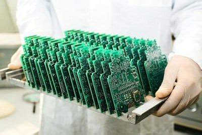
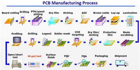
5. Manufacturing and Assembly Constraints
5.1 Component Spacing
- SMD and Through-Hole Clearances: Follow manufacturer-recommended spacing to avoid soldering defects.
- Pick-and-Place Considerations: Ensure adequate space for automated assembly equipment.
5.2 Testability and Debugging
- Test Points: Include accessible test points for critical signals to facilitate debugging.
- Silkscreen Markings: Clearly label component orientations and pin-1 indicators to avoid assembly errors.
Conclusion
Designing PCBs with special components demands a thorough understanding of electrical, thermal, and mechanical constraints. High-frequency components require controlled impedance and shielding, while high-power devices need robust thermal management. Precision analog circuits must be isolated from noise sources, and electromechanical components require careful placement for reliability. By adhering to these best practices, engineers can optimize performance, enhance manufacturability, and ensure long-term reliability in complex PCB designs.