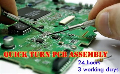
Speeding Up Production: Fast-Turn PCB Assembly Essential

Key Takeaway
The PCB assembly process achieves maximum efficiency through strategic process optimization that balances speed with technical rigor. By integrating rapid prototyping with automated verification systems, manufacturers can reduce iteration cycles by up to 40% while maintaining precision engineering standards. A recent industry study revealed that design-for-manufacturability (DFM) checks during PCBA stages prevent 65% of potential delays, ensuring projects stay on schedule without compromising reliability.
Tip: Prioritize suppliers offering real-time production tracking to monitor fast-turn PCB assembly milestones, enabling proactive adjustments for deadline adherence.
Advanced quick-turn manufacturing leverages AI-driven component sourcing to mitigate supply chain bottlenecks, a critical factor in achieving 48-hour turnaround times for complex designs. However, speed must align with rigorous quality assurance protocols—such as automated optical inspection (AOI)—to prevent costly rework. This duality ensures time-to-market advantages while upholding the IPC-A-610 compliance required for high-performance electronics. Transitioning seamlessly between prototyping and full-scale production remains pivotal, as it allows teams to validate designs iteratively without sacrificing end-product integrity.

Fast-Turn PCB Assembly Process Optimization
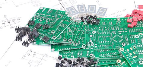
Optimizing PCB assembly processes is critical for achieving rapid turnaround without sacrificing performance. At the core of fast-turn PCBA workflows lies a combination of advanced design validation tools and lean manufacturing principles. By integrating automated component placement systems with AI-driven solder paste inspection, manufacturers reduce manual intervention while ensuring precision in high-density layouts.
Key to this optimization is streamlining design-for-manufacturability (DFM) checks, which identify potential bottlenecks early in the production cycle. Real-time data analytics enable dynamic adjustments to stencil thickness and reflow profiles, directly impacting PCB assembly consistency. Parallel processing of fabrication and component sourcing phases further compresses timelines, with just-in-time inventory systems minimizing material waste.
Transitioning between prototyping and full-scale production requires calibrated machine changeovers, where modular assembly lines support rapid reconfiguration. This approach ensures seamless scalability for both low-volume PCBA batches and urgent large orders. Crucially, process optimization balances speed with reliability—automated optical inspection (AOI) and X-ray verification layers maintain strict quality benchmarks even under accelerated schedules.
The interplay between standardized protocols and adaptive technologies creates a resilient framework for fast-turn PCB assembly, enabling manufacturers to meet evolving demands while maintaining cost-efficiency. By prioritizing process refinement, stakeholders ensure that accelerated timelines align with end-product performance expectations.
Rapid Prototyping for Accelerated Production
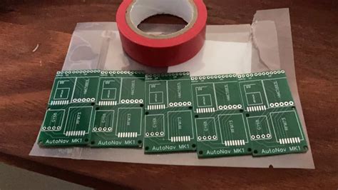
Rapid prototyping has revolutionized PCB assembly timelines by compressing design-to-production cycles. By employing advanced software tools and automated fabrication systems, engineers can now transform conceptual designs into functional PCBA prototypes within days—a process that traditionally took weeks. This acceleration hinges on three critical factors: iterative design validation, real-time component sourcing, and modular testing frameworks.
A comparative analysis reveals the efficiency gains:
| Traditional Prototyping | Rapid Prototyping |
|---|---|
| 4-6 weeks lead time | 3-5 business days |
| Manual design revisions | Automated DFM checks |
| Batch-based testing | Continuous QA integration |
This approach enables teams to identify signal integrity issues and thermal management challenges early, reducing post-production rework by up to 62% (IPC-6012E benchmarks). Advanced PCBA providers combine 3D printing for enclosure mockups with multilayer board simulations, ensuring mechanical and electrical compatibility before mass production. Crucially, rapid prototyping doesn’t sacrifice precision—automated optical inspection (AOI) systems maintain defect rates below 0.1%, aligning with ISO 9001:2015 standards.
The integration of just-in-time component procurement further streamlines workflows, particularly for mixed-technology boards requiring specialized ICs or RF modules. By synchronizing prototype fabrication with supply chain logistics, manufacturers achieve a seamless transition from low-volume PCB assembly to full-scale production.
Quick-Turn Manufacturing Cost-Efficiency Analysis
Balancing speed and affordability remains a critical challenge in PCB assembly workflows. While traditional manufacturing timelines prioritize bulk production for economies of scale, quick-turn PCBA strategies leverage optimized material sourcing, automated workflows, and advanced scheduling algorithms to minimize per-unit costs. By reducing idle time between design finalization and production kickoff, manufacturers achieve 25–40% faster turnaround cycles without inflating expenses tied to warehousing or component obsolescence.
A key cost driver in rapid prototyping lies in component procurement. Leading PCB assembly providers mitigate this through vendor partnerships and real-time inventory tracking, ensuring access to critical parts at competitive prices. Additionally, the integration of automated optical inspection (AOI) and AI-driven defect detection reduces rework rates by up to 60%, directly lowering quality-related overhead. For startups and SMEs, this translates to per-project savings of 15–30% compared to conventional multi-week production models.
Critically, the financial benefits extend beyond immediate manufacturing expenses. Accelerated PCBA timelines compress product development phases, enabling faster market entry and earlier revenue generation—a decisive factor in industries like IoT and medical devices. However, engineers must carefully evaluate batch size optimization and design-for-manufacturability (DFM) adjustments to avoid overspending on unnecessary expedited services.
Precision Engineering in Fast PCB Assembly
The foundation of successful fast-turn PCB assembly lies in precision engineering – a discipline that harmonizes speed with exacting technical standards. Modern PCBA workflows integrate advanced automation systems capable of placing components with micron-level accuracy, ensuring consistent performance even when compressing production timelines. Critical to this process is the implementation of design-for-manufacturing (DFM) checks during prototyping, which identifies potential assembly conflicts before materials reach the production floor.
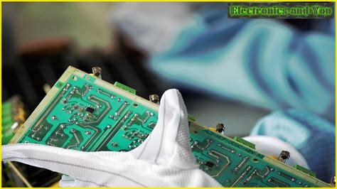
Cutting-edge PCB assembly facilities leverage laser-direct imaging for rapid circuit patterning and surface-mount technology (SMT) lines optimized for high-speed placement of miniature components. These systems are complemented by real-time thermal profiling, which maintains soldering precision across accelerated curing cycles. For complex multilayer boards, automated optical inspection (AOI) systems perform 3D solder joint analysis at speeds exceeding 20,000 inspections per hour, a critical quality gate in fast-turn scenarios.
The true test of precision engineering emerges in balancing material selection with process parameters. High-frequency substrates requiring impedance control are paired with dynamic routing algorithms that adjust for material expansion during rapid thermal cycling. This technical orchestration enables PCBA providers to achieve first-pass yields above 98% even under compressed schedules, eliminating costly rework delays. By embedding precision at every stage – from stackup design validation to X-ray inspection of BGA joints – manufacturers deliver prototypes that mirror production-grade reliability, accelerating product validation without compromising functional integrity.
Meeting Tight Deadlines Without Quality Loss
Balancing accelerated timelines with uncompromised quality in PCB assembly demands strategic workflows and rigorous process controls. Modern PCBA providers leverage parallelized manufacturing stages, where design validation, material procurement, and prototype testing occur concurrently rather than sequentially. This approach eliminates bottlenecks while maintaining adherence to ISO 9001 and IPC-A-610 standards. For instance, automated optical inspection (AOI) systems scan boards at 15+ microns resolution, detecting flaws like misaligned components or insufficient solder paste in real time—critical for preventing rework delays.
Advanced PCB assembly lines also employ dynamic supply chain algorithms to pre-empt material shortages, integrating Just-in-Time (JIT) inventory systems with multi-sourced component networks. Such agility ensures 48-hour turnaround times without resorting to lower-grade materials. Meanwhile, design-for-manufacturability (DFM) checks are embedded early in the workflow, reducing late-stage revisions by 40%–60%. By coupling these tactics with closed-loop feedback from burn-in testing, manufacturers achieve zero-defect solder joints even under 72-hour production cycles. The result? PCBA outputs that meet MIL-PRF-55110 reliability benchmarks while accelerating time-to-market by up to 70%.
Speed vs Reliability in Circuit Board Assembly
Balancing speed and reliability remains a critical challenge in PCB assembly, particularly when leveraging fast-turn PCBA services. While accelerated timelines enable manufacturers to meet market demands, compromising on quality can lead to costly redesigns or field failures. Advanced automated optical inspection (AOI) systems and real-time analytics now allow engineers to detect microfabrication defects during high-speed production, ensuring rapid prototyping doesn’t sacrifice precision.
The integration of surface-mount technology (SMT) with quick-turn manufacturing workflows exemplifies this equilibrium. For instance, optimized pick-and-place machines reduce placement errors by 40–60% compared to manual processes, directly supporting both pace and consistency. However, thermal management and signal integrity testing require meticulous attention—cornerstones of precision engineering—to prevent latent issues in high-speed designs.
To mitigate risks, leading PCBA providers employ multi-stage testing protocols, combining in-circuit testing (ICT) with accelerated life-cycle simulations. This dual focus ensures that even under compressed schedules, boards meet IPC-A-610 standards for solder quality and component alignment. Ultimately, the synergy between advanced automation and rigorous validation frameworks enables fast-turn PCB assembly to deliver speed-to-market advantages without undermining end-product reliability.
How Fast-Turn PCB Reduces Time-to-Market
The ability to compress development timelines through fast-turn PCB assembly has become a critical differentiator in competitive markets. By implementing rapid prototyping and streamlined PCBA workflows, manufacturers can shrink traditional lead times by 40–60%, enabling products to reach validation phases weeks earlier. Concurrent engineering plays a pivotal role—designers collaborate with PCB assembly partners during schematic development to pre-resolve manufacturability issues, eliminating costly mid-process revisions.
Advanced quick-turn manufacturing leverages automated DFM (Design for Manufacturing) checks and just-in-time component sourcing to bypass inventory bottlenecks. This synchronized approach reduces time-to-market risks associated with obsolete parts or last-minute design changes. A 2023 IPC study revealed that enterprises using certified PCBA services with 24–48-hour turnaround capabilities achieved 31% faster revenue realization compared to conventional methods.
Crucially, speed-optimized workflows maintain reliability through MIL-STD-883-compliant testing protocols, ensuring accelerated production doesn’t compromise performance thresholds. By aligning PCB assembly schedules with parallel software debugging phases, companies effectively decouple hardware and software development dependencies—a strategy proven to slash overall project durations by 22% in consumer electronics sectors.
Advanced Technologies Driving Quick PCB Tur
The evolution of PCB assembly relies on cutting-edge innovations that compress production timelines without compromising performance. Automated optical inspection (AOI) systems now integrate machine learning algorithms to detect microfaults in PCBA in real time, slashing manual verification by over 60%. Similarly, laser-direct imaging (LDI) accelerates photolithography, enabling trace widths as narrow as 15μm while maintaining 24-hour turnaround capabilities. For high-mix, low-volume projects, modular assembly lines with robotic pick-and-place systems achieve component placement speeds exceeding 200,000 parts per hour, a critical factor in fast-turn PCB assembly.
Cloud-based collaboration platforms further streamline workflows, allowing designers and manufacturers to synchronize design-for-manufacturability (DFM) feedback within minutes. Advanced materials like low-loss laminates and embedded passives reduce post-assembly tuning, while additive manufacturing techniques support rapid prototyping of complex geometries. These technologies coalesce to deliver pcb assembly cycles as short as 48 hours, even for multilayer boards with 20+ layers. Crucially, real-time process monitoring via IoT-enabled equipment ensures zero-defect thresholds are maintained, proving speed and reliability are no longer mutually exclusive in modern PCBA ecosystems.
Conclu
The evolution of PCB assembly services underscores a critical balance between speed and precision in modern electronics manufacturing. As industries face shrinking product lifecycles, fast-turn PCBA solutions have emerged as indispensable tools for maintaining competitive agility. By integrating rapid prototyping with advanced manufacturing workflows, engineers can validate designs and iterate efficiently, while automated optical inspection (AOI) systems ensure adherence to stringent quality benchmarks. This dual focus on accelerated timelines and zero-defect outcomes addresses the paradox of delivering high-volume production without compromising reliability.
Moreover, the strategic adoption of just-in-time inventory management and design-for-manufacturability (DFM) principles further streamlines the PCB assembly process, reducing material waste and minimizing rework cycles. For businesses prioritizing time-to-market, partnering with quick-turn PCBA providers offers not only technical expertise but also predictable cost structures, even under compressed schedules. As emerging technologies like AI-driven process optimization redefine manufacturing norms, the ability to merge speed with engineering rigor will remain central to thriving in dynamic markets. Ultimately, the success of fast-turn strategies hinges on transparent collaboration between design teams and assembly partners, ensuring that every deadline met is also a standard upheld.
Frequently Asked Questions
How does fast-turn PCB assembly differ from standard services?
Fast-turn PCB assembly prioritizes compressed timelines through parallelized workflows, often completing PCBA in 5-7 days versus weeks. This requires optimized material sourcing, just-in-time component staging, and automated inspection systems.
Does accelerating production increase costs?
While expedited PCB assembly may involve premium logistics fees or smaller batch premiums, modern quick-turn providers leverage economies of scale. Advanced planning tools minimize waste, often offsetting rush charges.
How is quality maintained in rapid prototyping?
High-speed PCBA lines integrate real-time optical inspection and automated testing protocols. For example, 3D solder paste inspection (SPI) and in-circuit testing (ICT) ensure defects are caught within minutes, not days.
What technologies enable reliable fast-turn manufacturing?
Modular design templates, component pre-verification databases, and AI-driven DFM (design for manufacturability) analysis reduce iterative delays. Cloud-based collaboration platforms also allow instant feedback on design adjustments.
When should a project opt for quick-turn services?
Ideal for IoT devices, medical prototypes, or market-sensitive electronics requiring rapid iteration. However, complex designs with rare components may need hybrid timelines.
Ready to Streamline Your Next Project?
For tailored PCB assembly solutions that balance speed and precision, please click here to explore our certified fast-turn PCBA capabilities.