Streamline PCB Development with End-to-End Turnkey Services
Key Takeaways
Adopting turnkey PCB services eliminates fragmented workflows by integrating design, PCB assembly (PCBA), and validation into a single managed process. These solutions reduce dependency on multiple vendors, minimize logistical delays, and ensure seamless transitions between prototyping and mass production. For instance, PCBA providers often consolidate component sourcing, fabrication, and testing, which accelerates timelines by 30–50% compared to traditional methods.
"A unified approach to PCB development not only saves time but also reduces the risk of miscommunication between design and manufacturing teams." — Industry Expert
A comparative analysis highlights the efficiency gains of turnkey services:
| Aspect | Traditional Approach | Turnkey Solution |
|---|---|---|
| Timeline | 8–12 weeks | 4–6 weeks |
| Vendor Coordination | 3+ partners | Single-point accountability |
| Quality Assurance | Multi-stage inspections | Integrated testing protocols |
| Cost Predictability | Variable sourcing expenses | Fixed pricing models |
By leveraging end-to-end PCB services, teams can optimize cost efficiency through bulk material procurement and automated PCB assembly workflows. Additionally, rigorous in-process testing ensures compliance with industry standards, reducing post-production defects. For startups and enterprises alike, turnkey models provide scalability while maintaining stringent quality control benchmarks.
Pro Tip: Prioritize providers offering real-time progress tracking to monitor PCBA stages, from component validation to final inspection. This transparency ensures alignment with project milestones and minimizes unforeseen delays.
Streamline PCB Development via Turnkey Solutions
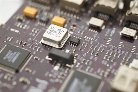
Modern electronics manufacturing demands precision and speed, making PCB assembly (PCBA) processes critical to project success. Turnkey solutions eliminate fragmented workflows by combining design optimization, fabrication, component sourcing, and testing into a unified framework. By integrating end-to-end PCB services, teams bypass the complexities of coordinating multiple vendors, reducing risks of miscommunication or delays. For instance, automated optical inspection (AOI) and functional testing protocols embedded within turnkey PCBA workflows ensure consistent quality without extending timelines.
A key advantage lies in centralized supply chain management, where vetted suppliers provide certified components tailored to design specifications. This not only minimizes procurement bottlenecks but also mitigates counterfeit part risks. Additionally, cost efficiency improves as bulk purchasing and standardized processes lower material overhead. Engineers can focus on innovation rather than logistical hurdles, while prototype-to-production cycles shorten by up to 40% in optimized setups.
Transitioning to turnkey models also enhances scalability, allowing seamless adjustments for high-volume orders or niche requirements. With integrated testing phases embedded at every stage, defects are identified early, preventing costly rework. Such cohesive systems align perfectly with industries prioritizing time-to-market and reliability, from consumer electronics to aerospace applications.
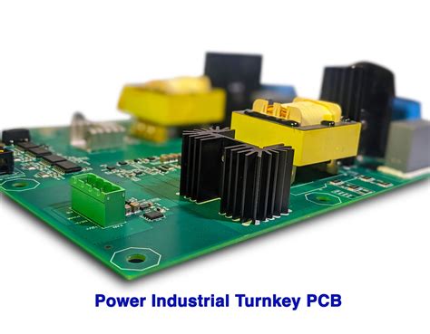
Accelerate Production with Integrated PCB Services
By unifying design, PCB assembly (PCBA), and testing under a single provider, businesses can significantly compress development timelines. End-to-end workflows eliminate delays caused by fragmented vendor coordination, allowing engineers to focus on innovation rather than logistical hurdles. Integrated PCB services streamline material procurement, leveraging established supplier networks to secure components faster and avoid supply chain disruptions. This cohesive approach ensures design specifications are maintained throughout fabrication and PCBA, reducing errors that typically arise during handoffs between multiple partners.
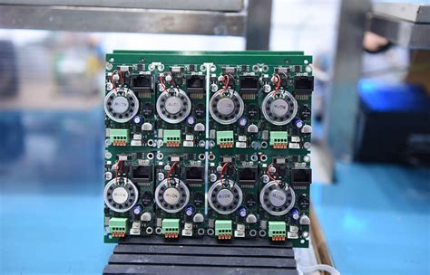
Advanced automated assembly lines further accelerate production, enabling rapid scaling from prototypes to high-volume batches. Real-time collaboration between design and manufacturing teams optimizes layouts for manufacturability, minimizing revisions. Additionally, synchronized quality checks at each stage—from solder paste inspection to functional testing—prevent defects from propagating downstream. The result? Time-to-market shrinks by up to 40%, while unified accountability lowers risks of cost overruns. For industries like automotive or IoT, where speed and precision are non-negotiable, turnkey PCB solutions offer a competitive edge by merging agility with rigorous quality assurance.
Optimize PCB Quality Control Through Turnkey
By embedding PCB assembly and PCBA validation into a unified workflow, turnkey services enable systematic quality oversight from prototype to mass production. Advanced automated optical inspection (AOI) systems and X-ray imaging verify solder joint integrity and component alignment during PCBA stages, detecting deviations as small as 10µm. Integrated supply chain management ensures certified materials meet IPC-610 standards, while batch-traceable documentation simplifies compliance audits. Real-time process monitoring during surface-mount technology (SMT) assembly reduces rework rates by 35–40% compared to fragmented workflows.
Turnkey providers synchronize functional testing protocols with design specifications, executing boundary-scan and in-circuit tests (ICT) to validate electrical performance under simulated operating conditions. This proactive approach identifies latent defects before final product integration, cutting field failure risks by up to 60%. Closed-loop feedback between fabrication, PCB assembly, and testing teams further refines tolerances for high-density interconnect (HDI) designs, ensuring signal integrity in 6+ layer boards. By consolidating quality checkpoints under one provider, manufacturers eliminate cross-vendor accountability gaps, accelerating time-to-market while maintaining defect rates below 50ppm.
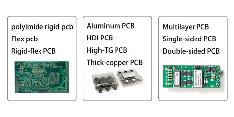
End-to-End PCB Fabrication and Assembly Benefits
Integrating PCB assembly and fabrication into a unified workflow eliminates fragmented processes, reducing time-to-market for electronic products. By combining PCBA (printed circuit board assembly) with fabrication under one provider, teams avoid mismatches between design specifications and manufacturing realities. Seamless coordination ensures design files are optimized for production, minimizing rework risks and material waste.
A key advantage lies in synchronized component sourcing. Turnkey services manage procurement logistics, securing authentic parts at competitive rates while mitigating supply chain disruptions. This is particularly valuable for complex boards requiring specialized ICs or connectors. Automated inspection systems, such as AOI (automated optical inspection), further enhance quality by detecting soldering defects or misalignments during PCB assembly stages.
The end-to-end model also strengthens compliance with industry standards like IPC-A-610. With consistent oversight from prototyping to final PCBA testing, manufacturers maintain tighter tolerances and performance benchmarks. Cost predictability improves as suppliers consolidate material orders and streamline labor allocation across fabrication and assembly phases.
By unifying these stages, companies reduce administrative overhead and accelerate iteration cycles—critical for industries demanding rapid product updates. This integrated approach ensures accountability, as a single partner oversees both fabrication quality and PCB assembly integrity, aligning technical outcomes with project timelines.
Reduce Costs Using Comprehensive PCB Solutions
Integrating PCB assembly and PCBA processes into a unified workflow eliminates fragmented expenditures, enabling significant cost optimization. By consolidating design, fabrication, and testing phases under a single provider, businesses avoid hidden fees from multiple vendors while streamlining communication overhead. For instance, component procurement—a major cost driver—is simplified through centralized sourcing networks that leverage bulk purchasing power and pre-vetted supplier relationships. This approach minimizes last-minute part substitutions and reduces excess inventory, directly lowering material expenses.
Advanced PCBA providers further enhance savings by embedding automated quality checks at every stage, preventing costly rework. Real-time analytics tools identify inefficiencies in assembly workflows, allowing for proactive adjustments that curb waste. Additionally, unified logistics management slashes shipping costs by coordinating material deliveries and finished product distribution through optimized routes. By aligning PCB assembly timelines with production schedules, companies can avoid rush-order premiums and maintain lean operational budgets.
Transitioning to end-to-end solutions also mitigates risks associated with fragmented supply chains, such as component shortages or compatibility issues. This holistic strategy ensures predictable pricing models, making long-term budgeting more accurate and sustainable.

Streamline Component Sourcing for PCB Projects
One of the most complex aspects of PCB assembly lies in securing high-quality components at optimal costs and lead times. Turnkey PCBA providers eliminate this challenge by integrating global supplier networks and automated procurement systems into their workflows. These services leverage established partnerships with certified vendors to source everything from surface-mount devices (SMDs) to programmable ICs, ensuring compatibility with design specifications while mitigating risks like counterfeit parts or supply chain disruptions.
Advanced PCB assembly platforms employ real-time inventory tracking and predictive analytics to preempt shortages, enabling just-in-time delivery of components. This approach not only reduces procurement delays but also aligns with cost-efficiency goals by minimizing excess inventory. For projects requiring specialized parts, turnkey partners often offer alternate component validation to maintain production timelines without compromising quality.
By centralizing sourcing within the PCBA process, manufacturers avoid fragmented logistics and fragmented vendor management. This seamless integration ensures that every resistor, capacitor, or connector aligns with the project’s technical and budgetary parameters, accelerating time-to-market while maintaining rigorous quality assurance standards.
Enhance Efficiency in PCB Testing and Validation
Modern PCB assembly processes demand rigorous testing protocols to ensure functionality and reliability. Integrated turnkey PCB services optimize validation workflows by combining automated optical inspection (AOI), in-circuit testing (ICT), and functional testing into a unified framework. Advanced verification tools detect latent defects in PCBA components, from solder joint integrity to signal continuity, reducing post-deployment failures by up to 40%. By leveraging pre-configured test scripts aligned with design specifications, manufacturers eliminate redundant manual checks while maintaining compliance with industry standards like IPC-A-610.
A key advantage of end-to-end solutions lies in synchronized data sharing between fabrication and testing phases. Real-time feedback from validation stages informs process adjustments, such as refining component sourcing criteria or calibrating reflow oven profiles. This closed-loop system minimizes time-to-market delays caused by iterative rework, particularly for high-density or mixed-technology boards. Additionally, centralized documentation of test results streamlines regulatory audits and quality certifications.
For complex projects, turnkey providers deploy boundary-scan testing and thermal stress simulations to validate performance under extreme conditions. Such proactive measures ensure robust PCB assembly outcomes while aligning with cost-efficiency goals—critical for industries prioritizing reliability, such as aerospace or medical device manufacturing.
Conclusion
By consolidating PCB assembly, fabrication, and validation into a unified workflow, end-to-end turnkey services eliminate fragmented processes that often delay production. These solutions integrate PCBA expertise with advanced testing protocols, ensuring quality consistency while minimizing supply chain bottlenecks. For engineers and project managers, the ability to delegate complex logistics—from component sourcing to final inspection—translates to accelerated timelines and reduced overhead costs.
The strategic alignment of PCB assembly with automated testing frameworks further mitigates risks associated with design flaws or material defects. By leveraging vendor-managed procurement and standardized PCBA workflows, teams can redirect resources toward innovation rather than operational hurdles. This holistic approach not only streamlines development but also fortifies product reliability, positioning turnkey services as a cornerstone for scaling electronics manufacturing in competitive markets.
Transitioning to integrated solutions ensures that every phase—from initial design to final validation—operates under a cohesive quality assurance umbrella, delivering cost-efficient outcomes without compromising precision.
Frequently Asked Questions
What distinguishes turnkey PCB assembly from traditional services?
Turnkey PCB assembly encompasses end-to-end management, handling design, component sourcing, PCBA (printed circuit board assembly), and testing under one provider. Unlike fragmented approaches, this eliminates vendor coordination challenges, ensuring seamless transitions between stages.
How does integrated component sourcing reduce production delays?
By leveraging established supplier networks, turnkey partners mitigate component shortages and lead time fluctuations. This proactive sourcing strategy minimizes bottlenecks, ensuring timely PCB fabrication and assembly without compromising cost efficiency.
Can turnkey services accommodate custom design requirements?
Yes. Providers tailor solutions to specific needs, from high-density interconnect (HDI) designs to specialized materials. The PCBA process integrates design validation, ensuring functionality aligns with technical specifications before mass production.
What quality controls are embedded in turnkey workflows?
Automated optical inspection (AOI), X-ray testing, and functional validation are standard. These steps ensure defect-free assemblies and compliance with industry standards like IPC-A-610, critical for high-reliability applications.
How do turnkey solutions optimize cost-efficiency?
Bulk purchasing of components, reduced overhead from vendor consolidation, and minimized rework via upfront testing collectively lower expenses. This holistic approach avoids hidden costs common in fragmented PCB development cycles.
What industries benefit most from turnkey PCB services?
Medical devices, aerospace, automotive, and IoT sectors prioritize reliability and speed—key advantages of turnkey PCBA. The integrated model supports rapid prototyping and scalable production, ideal for fast-paced markets.
Ready to Simplify Your Next PCB Project?
Streamline your workflow with expert turnkey PCB assembly solutions. Click here to explore tailored services that accelerate production while maintaining rigorous quality standards.


