Streamlined Multi-Board Design Strategies for Affordable PCB Fabrication

Key Takeaways
When planning multi-board PCB manufacturing, understanding how design choices impact PCB manufacturing cost is crucial. Start by evaluating modular layouts that allow PCB manufacturing companies to process smaller, standardized boards efficiently—this approach often reduces material waste and accelerates assembly timelines. You’ll want to prioritize design for manufacturability (DFM) principles, such as consistent component placement and standardized connector systems, to avoid costly rework during fabrication.
Balancing space constraints with circuit integrity requires strategic partitioning: split complex circuits into functional blocks while maintaining signal integrity through controlled impedance routing. For budget-conscious projects, collaborate early with your PCB manufacturing business partner to align material choices (like FR-4 vs. high-frequency laminates) with cost targets. Transitioning to streamlined workflows—such as using unified design rules across modules—can further trim expenses by minimizing errors and revision cycles.
Don’t overlook testing: implement boundary scan or *automated optical inspection (https://www.andwinpcba.com) on balancing performance and affordability in modular systems.
Modular PCB Layouts for Cost-Efficient Assembly
When designing multi-board systems, adopting modular PCB layouts allows you to break complex circuits into reusable, standardized blocks. This approach simplifies assembly by enabling parallel production of individual modules, reducing PCB manufacturing costs associated with large, monolithic boards. By isolating functional blocks like power supplies or communication interfaces, you minimize cross-module interference while streamlining testing and repairs.
Tip: Work with PCB manufacturing companies early in the design phase to align module dimensions with their panelization standards. This avoids material waste and optimizes fabrication yield.
A key advantage lies in scalability: modular designs let you swap or upgrade components without redesigning the entire system. For instance, separating a microcontroller unit from sensor arrays allows independent updates, cutting long-term PCB manufacturing business expenses. However, ensure consistent signal integrity across connectors by maintaining controlled impedance traces and minimizing inter-board cabling.
To further reduce PCB manufacturing cost, standardize module footprints and layer stackups. This simplifies procurement and assembly workflows, as suppliers can batch-produce identical modules. Use design-for-manufacturing (DFM) checks to verify tolerances for split boards, preventing misalignment during final integration.
By balancing modularity with fabrication-friendly practices, you achieve cost-efficient assembly without compromising reliability—a critical balance for budget-driven projects.

Balancing Space Constraints in Multi-Board Designs
When designing multi-board systems, managing PCB manufacturing cost while addressing spatial limitations requires strategic planning. Start by analyzing the functional partitioning of circuits to avoid redundant components across boards. For instance, grouping high-frequency signals on a single module minimizes cross-talk risks and reduces the need for shielding on adjacent boards. This approach not only saves space but also streamlines assembly workflows for PCB manufacturing companies.
A common challenge is balancing board density with accessibility for testing and repairs. Overcrowding increases the likelihood of fabrication errors, which can escalate PCB manufacturing business expenses. To mitigate this, consider these strategies:
| Design Strategy | Space Impact | Cost Benefit |
|---|---|---|
| Vertical stacking with connectors | Reduces footprint by 30-40% | Lowers material usage by 15-20% |
| Flexible inter-board routing | Optimizes signal paths | Cuts layer count requirements |
| Shared power/ground planes | Minimizes board thickness | Reduces copper etching costs |
Collaborate early with PCB manufacturing partners to validate tolerances and material choices. For example, thinner substrates might save space but could compromise durability, increasing long-term PCB manufacturing cost. Use simulation tools to model thermal and mechanical stresses, ensuring designs remain robust under real-world conditions. By prioritizing modularity without sacrificing reliability, you create systems that align with both spatial and budgetary constraints.
Affordable Fabrication Techniques for Split PCBs
When designing split PCBs, balancing PCB manufacturing cost with performance starts with strategic partitioning. By dividing complex circuits into smaller, standardized modules, you simplify production workflows for PCB manufacturing companies, which often charge less for repetitive, panelized designs. Optimized board dimensions that align with standard panel sizes reduce material waste, while avoiding irregular shapes minimizes tooling adjustments during fabrication.
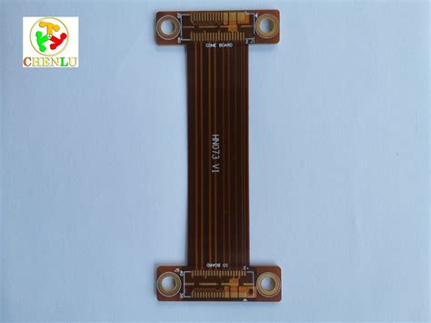
To further cut expenses, consider using V-groove or tab-route designs for clean separations, as these methods require fewer specialized processes compared to laser cutting. Partnering with PCB manufacturing businesses that offer volume discounts for multi-board orders can also lower per-unit costs. However, ensure your split points don’t compromise signal integrity—critical traces should remain on a single board to avoid cross-module interference.
Material selection plays a dual role here: thinner substrates (like 0.8mm FR-4) reduce weight and cost but require careful handling during assembly. Always validate your design with manufacturers early to align with their PCB manufacturing capabilities, avoiding last-minute revisions that inflate budgets. Finally, automated testing jigs for individual modules streamline quality checks, preventing costly rework in later stages.
Optimizing Circuit Integrity in Modular Board Systems
When implementing modular designs, maintaining circuit integrity becomes critical as signal paths span multiple boards. Start by analyzing signal propagation delays and cross-talk risks between interconnected modules. Use PCB manufacturing best practices like controlled impedance routing and ground plane partitioning to minimize interference. For high-speed signals, ensure impedance matching across board interfaces—mismatches here can degrade performance and increase PCB manufacturing cost due to rework.
A common pitfall is overlooking return path continuity in split designs. Always verify that ground connections remain uninterrupted between modules, even when boards are separated. This becomes particularly vital when working with PCB manufacturing companies that specialize in multi-board assemblies, as their fabrication tolerances directly impact signal reliability.
To balance cost and quality, employ simulation tools to model electromagnetic behavior before finalizing layouts. Techniques like guard traces or differential pairing can shield sensitive signals without inflating PCB manufacturing business expenses. Additionally, collaborate with fabricators early to align material choices (e.g., low-loss substrates) with both electrical requirements and budget constraints.
Finally, validate designs through rigorous testing protocols, such as boundary-scan checks or impedance verification, to catch integrity issues before mass production. By integrating these strategies, you ensure modular systems meet performance benchmarks while staying compatible with affordable PCB manufacturing workflows.
Material Selection for Budget-Friendly Multi-Board Projects
When designing multi-board systems, your choice of materials directly impacts PCB manufacturing cost and long-term reliability. Start by evaluating standard FR-4 substrates, which offer a balance of performance and affordability for most applications. For projects requiring thermal management or flexibility, consider cost-optimized alternatives like CEM-1 or aluminum-backed boards, but verify their compatibility with your PCB manufacturing business partner’s capabilities.
Collaborate early with PCB manufacturing companies to identify material grades that meet electrical requirements without over-specifying. For instance, mid-Tg FR-4 (140–150°C) often suffices for consumer electronics, avoiding the premium for high-Tg variants. Similarly, standard 1-ounce copper layers reduce PCB manufacturing complexity compared to thicker options, unless high-current traces demand it.
Leverage panelization strategies to minimize waste—selecting panel sizes that align with your fabricator’s equipment reduces material trimming costs. If using mixed materials across boards, ensure compatibility in thermal expansion coefficients to prevent warping during assembly. Finally, prioritize suppliers offering bulk pricing for prototype-grade laminates, as this lowers per-unit expenses without sacrificing critical performance parameters. By aligning material choices with both design goals and PCB manufacturing cost drivers, you create modular systems that remain economical at scale.
Streamlined Design Workflows for Reduced Assembly Costs
When optimizing PCB manufacturing workflows, focus on eliminating redundancies that inflate PCB manufacturing cost. Start by adopting standardized component libraries to reduce design iterations—this ensures compatibility with automated assembly processes used by most PCB manufacturing companies. Use design-for-manufacturing (DFM) principles early in layout planning, such as aligning component orientations and minimizing unique part numbers, to simplify pick-and-place operations.
Leverage software tools that automate trace routing and component placement, which cuts engineering hours while maintaining precision. For multi-board systems, employ modular design templates to reuse validated layouts across projects, reducing both development time and prototyping expenses. Collaborate with your PCB manufacturing business partner during the schematic phase to identify cost-saving opportunities, like panelization strategies that maximize material usage.
Finally, implement version control and centralized documentation to prevent errors during handoffs between design and production teams. By streamlining these workflows, you not only accelerate time-to-market but also create repeatable processes that scale efficiently—critical for managing PCB manufacturing cost in high-volume orders.
Testing Strategies for Reliable Multi-Board Integration
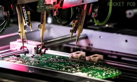
When integrating multiple boards, thorough testing ensures functional consistency across modules while addressing PCB manufacturing cost concerns. Start by validating individual board functionality through boundary scan testing (BST), which isolates faults in high-density interconnects without physical probes. For interconnected systems, employ automated optical inspection (AOI) to verify solder joint integrity and alignment accuracy—critical factors that PCB manufacturing companies prioritize for multi-board reliability.
Leverage cross-talk analysis tools during signal integrity testing to identify interference risks between adjacent modules, especially when working with budget-conscious PCB manufacturing business models. Implement impedance matching checks across split boards to maintain signal fidelity, reducing rework expenses. Partnering with PCB manufacturing specialists who offer panelized testing can further streamline quality assurance, as bulk verification of modular designs often lowers per-unit costs.
Finally, conduct system-level stress tests under real-world operating conditions. Thermal cycling and vibration simulations expose weak points in mechanical or electrical interfaces, allowing you to refine designs before full-scale production. By aligning these strategies with PCB manufacturing cost optimization goals, you ensure robust multi-board integration without compromising affordability.
Minimizing Fabrication Expenses with Smart Board Partitioning
When designing multi-board systems, strategic partitioning directly impacts PCB manufacturing cost by optimizing material usage and production efficiency. By dividing complex circuits into functional clusters, you reduce the need for oversized panels or specialized tooling, which often inflate expenses in PCB manufacturing business workflows. Start by analyzing signal flow and power requirements—grouping high-speed components or noise-sensitive circuits onto separate boards simplifies routing and minimizes cross-interference.
Collaborating with PCB manufacturing companies early in the design phase ensures your partitioning aligns with their standard panel sizes and assembly processes. For example, splitting a large board into smaller, identical modules allows manufacturers to maximize panel utilization, lowering per-unit material waste. However, avoid over-partitioning: excessive inter-board connectors or redundant circuitry can negate savings by increasing PCB manufacturing complexity.
Leverage modular symmetry to standardize sub-board dimensions, enabling batch fabrication of interchangeable units. This approach not only cuts prototyping costs but also streamlines scaling for future revisions. Additionally, consider mixed-technology splits—placing cost-sensitive analog sections on separate boards from high-density digital areas—to balance PCB manufacturing cost without compromising performance.
Finally, validate partitioning choices through simulation tools to identify thermal or signal integrity risks before committing to production. A well-partitioned design reduces rework cycles, ensuring your project stays within budget while meeting functional demands.
Conclusion
When designing multi-board systems for PCB manufacturing, the balance between affordability and performance hinges on strategic planning. By adopting modular design principles, you can simplify assembly processes while maintaining circuit integrity—a critical factor in reducing PCB manufacturing cost. Prioritize collaboration with experienced PCB manufacturing companies to leverage their expertise in material optimization and fabrication techniques tailored for split-board architectures.
Smart partitioning not only addresses space constraints but also streamlines testing phases, ensuring reliable integration across modules. This approach minimizes rework risks, which often inflate expenses in the PCB manufacturing business. Remember, selecting standardized components and panelization strategies further lowers per-unit costs without compromising quality.
Ultimately, the goal is to create a cohesive workflow that aligns design choices with fabrication realities. By focusing on scalable layouts and proactive communication with manufacturers, you can achieve cost-efficient production cycles that meet both technical and budgetary demands.
FAQs
How does multi-board design affect pcb manufacturing cost?
By splitting complex circuits into modular boards, you reduce panel waste and enable parallel assembly—key factors pcb manufacturing companies consider when pricing projects. Strategic partitioning often lowers material usage and simplifies testing, directly cutting pcb manufacturing expenses.
What design practices ensure reliability in multi-board systems?
Maintain consistent trace widths and spacing across modules to prevent impedance mismatches. Use standardized connectors validated by pcb manufacturing business experts, and prioritize signal integrity simulations to avoid costly post-fabrication fixes.
Can modular designs compromise circuit performance?
When planned carefully, modular systems preserve circuit integrity by isolating noise-sensitive components. Work with pcb manufacturing partners to validate board-to-board communication protocols and ensure EMI compliance without inflating pcb manufacturing cost.
How do space constraints influence board partitioning?
Balancing compact layouts with manufacturable module sizes requires iterative prototyping. Many pcb manufacturing companies offer design-for-manufacturing (DFM) feedback to optimize split points, ensuring panels fit standard fabrication equipment while minimizing material waste.
What materials best suit budget-friendly multi-board projects?
FR-4 substrates with mid-Tg ratings provide a cost-performance balance for most applications. For high-density interconnects, consider hybrid designs using low-cost base materials paired with selective pcb manufacturing upgrades like ENIG finishes on critical layers.
Explore Professional PCB Manufacturing Solutions
For tailored guidance on optimizing your multi-board project’s pcb manufacturing cost and reliability, please click here to consult industry experts.


