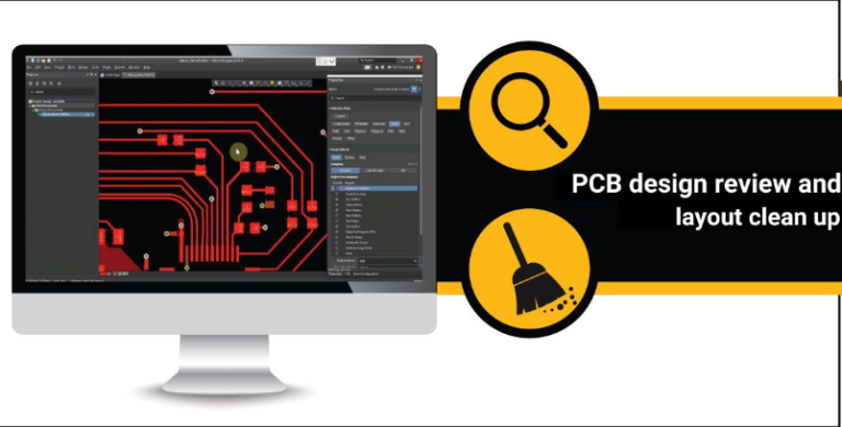
Streamlined Multilayer PCB Prototyping Techniques Unveiled

Key Takeaways
When navigating PCB manufacturing for multilayer prototypes, understanding cost drivers and technical trade-offs becomes critical. Leading PCB manufacturing companies now employ design-for-manufacturability (DFM) principles to reduce PCB manufacturing cost while maintaining signal integrity—especially for high-density interconnect (HDI) or rigid-flex designs.
"Prototyping success starts with selecting a partner that balances advanced capabilities with transparent pricing models. Ask for stack-up validation reports early to avoid impedance mismatches in high-frequency applications."
Three factors dominate modern PCB manufacturing business strategies:
| Factor | Impact on Prototyping | Cost Optimization Tip |
|---|---|---|
| Layer Count | Increases material usage and lamination cycles | Use hybrid constructions (mixed dielectrics) |
| Via Technology | Microvias reduce layer jumps but require laser drilling | Reserve HDI for critical RF sections |
| Surface Finish | ENIG adds $0.15/cm² but improves reliability | Apply selective gold plating only on connectors |
For rigid-flex designs, prioritize bend radius simulations to prevent copper fatigue—a common oversight that increases PCB manufacturing cost through re-spins. Advanced firms now combine automated optical inspection (AOI) with impedance testing, slashing defect rates by 37% compared to traditional methods.
When evaluating PCB manufacturing companies, verify their rapid-turn capabilities for:
- 24-hour multilayer processing (requires direct laser imaging systems)
- Panel utilization rates above 85% (reduces material waste)
- In-house via filling (eliminates third-party delays)
Tip: Always request a manufacturability scorecard—top-tier suppliers provide this breakdown showing how your design choices impact lead times and PCB manufacturing business margins.
For high-frequency boards, tight impedance control (±5%) becomes non-negotiable. This demands precise dielectric constant management, pushing many teams toward specialty substrates like Rogers 4350B. However, partnering with PCB manufacturing experts who stock niche materials can prevent 2-3 week procurement delays.
Remember: Streamlined prototyping isn’t just about speed—it’s about creating feedback loops where design iterations inform process improvements. Modern ERP systems in PCB manufacturing companies now track 14+ quality metrics per layer pair, enabling data-driven refinements across subsequent builds.

Rapid Multilayer PCB Prototyping
When accelerating PCB manufacturing timelines for multilayer designs, you need strategies that balance speed with uncompromised quality. Modern rapid prototyping leverages advanced technologies like laser direct imaging (LDI) and automated optical inspection (AOI) to shrink lead times to 24-48 hours for 4- to 12-layer boards. These methods enable PCB manufacturing companies to validate complex stack-ups—such as mixed-signal layouts or impedance-controlled traces—without sacrificing precision.
A critical factor in managing PCB manufacturing cost during prototyping lies in material selection. For instance, opting for FR-4 substrates with mid-range Tg values can reduce expenses while maintaining thermal stability for most applications. However, high-frequency designs often require specialized laminates like Rogers or Isola, which directly influence both performance and budget. To mitigate risks, many engineers use simulation tools to pre-validate signal integrity, minimizing iterative revisions that inflate costs.
For businesses scaling their PCB manufacturing business, integrating rigid-flex capabilities into prototyping workflows is becoming essential. Hybrid designs combining rigid and flexible sections demand precise layer alignment—a process streamlined through laser-drilled microvias and sequential lamination techniques. Partnering with manufacturers that offer design-for-manufacturability (DFM) checks ensures your prototypes adhere to production-ready standards, avoiding costly redesigns later.
Transitioning from prototype to volume production? Prioritize partners with agile scaling frameworks. For example, modular assembly lines allow seamless shifts between low-volume prototyping and high-output manufacturing, maintaining consistency across batches. This approach not only optimizes PCB manufacturing cost but also future-proofs your supply chain against fluctuating demand.
Ultimately, rapid multilayer PCB prototyping thrives on collaboration between designers and manufacturers. By aligning your design intent with fabrication realities early, you unlock faster iterations, fewer delays, and a clearer path to market readiness.

Cost-Effective Rigid-Flex PCBs
When designing rigid-flex PCBs, balancing performance and pcb manufacturing cost requires strategic planning. Unlike traditional rigid boards, rigid-flex designs integrate both flexible and rigid substrates, enabling compact layouts while reducing assembly complexity. To achieve cost efficiency, you must prioritize material selection and layer count optimization. For instance, using polyimide-based flex layers paired with FR-4 rigid sections can lower material expenses without compromising durability—a critical consideration for pcb manufacturing business models focused on high-volume production.
Leading pcb manufacturing companies often leverage advanced lamination techniques to minimize waste during fabrication. By adopting sequential bonding processes, they reduce the risk of delamination, which directly impacts yield rates and long-term reliability. Additionally, design-for-manufacturability (DFM) principles play a pivotal role. Simplifying bend radii and avoiding abrupt transitions between rigid and flexible zones not only enhances functionality but also streamlines assembly, further curbing pcb manufacturing expenses.
Another cost-saving strategy involves panel utilization. Maximizing the number of boards per panel reduces material waste, especially when working with pcb manufacturing partners that offer panel-sharing options. For prototypes or low-volume runs, opting for standardized flex materials and avoiding custom thicknesses can significantly lower upfront costs. However, it’s essential to collaborate closely with your manufacturer to validate design choices early—this prevents costly revisions during later stages.
For high-frequency or high-density applications, hybrid rigid-flex designs can replace multiple interconnected boards, eliminating connectors and solder joints that drive up pcb manufacturing cost. Advanced pcb manufacturing companies now employ laser drilling and automated optical inspection (AOI) to ensure precision in microvias and fine-pitch traces, which is vital for maintaining signal integrity in compact layouts.
Ultimately, achieving affordability in rigid-flex PCBs hinges on harmonizing design innovation with manufacturing pragmatism. By aligning your specifications with proven pcb manufacturing workflows, you can unlock scalable solutions that meet both technical and budgetary demands.
HDI Board Manufacturing Advances
Modern PCB manufacturing now integrates high-density interconnect (HDI) technologies to meet the escalating demand for compact, high-performance electronics. Leading PCB manufacturing companies leverage laser drilling and stacked microvia architectures to achieve trace widths as narrow as 25μm, enabling up to 20 layers in designs no thicker than 1.6mm. These advancements directly address PCB manufacturing cost challenges by reducing material waste through automated optical inspection (AOI) and design-for-manufacturability (DFM) optimizations.
For your projects requiring ultra-fine pitch components, sequential lamination processes now support hybrid builds combining rigid and flexible substrates—a critical feature for wearables and medical devices. By adopting modified semi-additive processes (mSAP), fabricators achieve 30% higher yield rates compared to traditional subtractive methods, making high-volume HDI production viable even for mid-scale PCB manufacturing business operations.
Transitioning to HDI doesn’t just enhance performance; it redefines thermal management. Copper-filled microvias and embedded passive components dissipate heat 40% more efficiently than conventional through-hole vias, extending product lifespans in automotive and aerospace applications. To maintain competitiveness, prioritize partners offering direct imaging systems and real-time impedance control, which slash prototyping cycles from weeks to days while ensuring ±5% signal integrity tolerances.
As you evaluate HDI solutions, consider how low-loss dielectric materials like Megtron 6 or Isola FR408HR reduce insertion losses by up to 0.002 dB/cm at 10 GHz—essential for 5G infrastructure. This strategic alignment between advanced materials and precision engineering allows PCB manufacturing companies to deliver 0.15mm pitch BGAs without compromising reliability, even when operating at -55°C to 150°C extremes. By mastering these innovations, your team can bypass traditional PCB manufacturing cost barriers while scaling complex multilayer designs with military-grade durability.

High-Frequency PCB Techniques
When designing high-frequency PCBs, signal integrity becomes paramount. These boards, often used in RF communications, radar systems, and 5G infrastructure, demand specialized techniques to minimize signal loss and electromagnetic interference (EMI). Low-loss dielectric materials like Rogers or Taconic laminates are critical here, as they maintain stable permittivity at high frequencies while reducing parasitic capacitance.
PCB manufacturing companies leverage advanced simulation tools to model impedance control, ensuring trace geometries and dielectric thickness align with target frequencies. For instance, microstrip or stripline configurations are optimized to handle GHz-range signals without degradation. This precision directly impacts PCB manufacturing cost, as tighter tolerances require higher-grade materials and more rigorous testing protocols.
Thermal management also plays a vital role. High-frequency circuits generate significant heat, which can destabilize performance if not properly dissipated. Copper weights and via structures are carefully calibrated to balance conductivity and thermal expansion coefficients. Some PCB manufacturing businesses integrate embedded heat sinks or metal-core substrates for applications like satellite transceivers, where reliability under thermal stress is non-negotiable.
Another key consideration is surface finish selection. Electroless nickel immersion gold (ENIG) is often preferred over HASL for high-frequency boards due to its smoother surface, which reduces skin effect losses at elevated frequencies. Additionally, PCB manufacturing workflows now incorporate laser-drilled microvias to minimize parasitic inductance in HDI designs, a technique that dovetails with the demands of high-frequency layouts.
To mitigate crosstalk, designers employ isolation techniques such as grounded coplanar waveguides or shielding cans. Partnering with PCB manufacturing companies that specialize in RF prototyping ensures access to vector network analyzers (VNAs) and time-domain reflectometry (TDR) for real-world validation. This collaboration bridges the gap between theoretical models and physical board performance, a critical step in avoiding costly redesigns.
By integrating these methodologies, you achieve boards that meet stringent signal integrity requirements while balancing PCB manufacturing cost and lead times—a necessity in industries where both precision and speed define competitive advantage.

Streamlined Production Processes
Modern PCB manufacturing relies on digitally integrated workflows to eliminate bottlenecks while maintaining precision. Leading PCB manufacturing companies now deploy automated optical inspection (AOI) systems paired with real-time data analytics, reducing manual verification steps by up to 70%. This approach not only accelerates prototyping cycles but also minimizes human error—critical for multilayer boards with 12+ layers or microvia architectures.
To address PCB manufacturing cost concerns, advanced firms employ design-for-manufacturability (DFM) checks early in the process. By simulating production outcomes during the design phase, you avoid costly post-fabrication revisions. For instance, automated layer stackup optimization tools can slash material waste by 22% in high-frequency designs while ensuring impedance control tolerances stay within ±5%.
The PCB manufacturing business has shifted toward modular tooling configurations that enable rapid transitions between rigid-flex and HDI prototypes. Laser direct imaging (LDI) systems, combined with adaptive plating lines, allow manufacturers to switch from 6-layer FR-4 boards to 20-layer hybrid builds in under 48 hours. This flexibility is particularly valuable when iterating antenna-in-package designs or millimeter-wave circuits requiring precise dielectric constant management.
Smart factory integration further streamlines operations through machine learning-driven yield prediction. By analyzing historical production data, systems preemptively flag potential defects in buried capacitance layers or staggered via structures—reducing scrap rates by up to 18%. Such advancements let you balance speed with reliability, even when dealing with ultra-low-loss materials like Rogers 4350B for 5G applications.
Transitioning to these methods requires aligning with partners who prioritize closed-loop process control. This ensures thermal management features in power electronics or impedance-matched traces for RF boards meet specifications without requiring multiple prototype iterations. The result? A seamless bridge between complex design intent and mass production readiness.
Precision PCB Engineering
Achieving sub-10-micron accuracy in PCB manufacturing requires balancing technical expertise with advanced process controls. When developing multilayer prototypes, you need partners capable of maintaining tightest impedance tolerances (±2%) while managing PCB manufacturing cost through material optimization. Modern PCB manufacturing companies employ laser-direct imaging (LDI) systems to achieve ±1.5 mils trace width consistency, critical for high-speed digital and RF designs.
This precision extends beyond component placement—it demands three-dimensional alignment of inner-layer cores during lamination, particularly for 12+ layer stacks. Thermal stress simulations prevent warpage in high-Tg materials, ensuring reliability across operating temperatures. Prototyping phase data directly informs volume production setups, making collaboration with PCB manufacturing business specialists essential for scaling without quality loss.
Advanced DFM checks now integrate AI-driven error prediction algorithms, reducing re-spins by 38% in recent industry benchmarks. You’ll want suppliers offering automated optical inspection (AOI) with 25μm resolution and cross-sectional microsection analysis—key tools for verifying blind/buried via fill quality in HDI designs. For impedance-critical applications like 5G infrastructure, look for pre-production simulations correlating dielectric properties with actual test coupons.
Cost containment strategies focus on panel utilization optimization and layer stack mirroring techniques. However, cutting corners on copper surface roughness (≤0.3μm Ra for mmWave PCBs) or via wall uniformity risks signal integrity. Leading firms offset PCB manufacturing cost through hybrid pricing models—volume commitments for base materials paired with flexible NRE charges for prototype engineering.
The most efficient PCB manufacturing companies streamline this complexity using digital twin workflows, where design files synchronize with production equipment in real time. This approach slashes setup errors by 67% while maintaining ±0.075mm layer-to-layer registration—a non-negotiable for aerospace-grade rigid-flex assemblies. Through strategic partnerships, you gain access to these precision tools without upfront capital investments, turning engineering challenges into competitive advantages.
Advanced Prototyping Solutions
When developing complex electronic systems, you need PCB manufacturing partners capable of translating intricate designs into functional prototypes without compromising speed or accuracy. Modern advanced prototyping solutions leverage automated design validation tools and multi-layer stacking technologies to address challenges like signal integrity and thermal management. Leading PCB manufacturing companies now employ hybrid workflows combining 3D printing for rapid layer alignment with laser direct imaging (LDI) for micron-level precision, slashing turnaround times by up to 40% compared to traditional methods.
A critical consideration is balancing PCB manufacturing cost with performance requirements. For high-density interconnect (HDI) boards, sequential build-up (SBU) processes enable tighter via spacing while minimizing material waste. Advanced simulation software predicts impedance mismatches early, reducing iterative prototyping cycles. This approach proves particularly valuable for rigid-flex designs, where mechanical stress analysis ensures reliability across bending cycles.
To optimize your PCB manufacturing business case, consider modular prototyping platforms that support both FR4 and high-frequency laminates. These systems allow parallel testing of different material configurations, accelerating time-to-market for RF and microwave applications. Some providers offer shared engineering models, granting access to specialized expertise in controlled impedance routing without upfront capital investments.
Transitioning from prototype to volume production requires seamless data integration between design and fabrication teams. Cloud-based DFM (design for manufacturing) platforms now provide real-time feedback on stackup feasibility, ensuring your multilayer prototypes align with scalable manufacturing workflows. By prioritizing manufacturability during the prototyping phase, you avoid costly redesigns while maintaining flexibility for last-minute specification changes.
Rigid-Flex Design Optimization
When optimizing rigid-flex PCB manufacturing designs, balancing mechanical reliability with electrical performance becomes critical. Dynamic bend areas require careful material selection—polyimide substrates are often preferred for their flexibility and thermal stability. To minimize PCB manufacturing cost, you’ll need to standardize layer counts where possible, as alternating rigid and flexible sections increases complexity. Leading PCB manufacturing companies recommend maintaining consistent bend radii (typically 6-10x the flex layer thickness) to prevent material fatigue during repeated flexing.
Transitioning from rigid to flexible zones demands precise adhesive selection and copper weight adjustments. For example, using rolled annealed copper in flex regions improves durability, while electro-deposited copper suits rigid sections. Signal integrity in high-speed applications depends on optimizing trace routing to avoid stress points—angled or curved traces outperform 90-degree turns. Collaborative design reviews with your PCB manufacturing business partner help identify potential fabrication issues early, such as mismatched coefficient of thermal expansion (CTE) between materials.
Thermal management also plays a role: rigid sections often integrate heatsinks, whereas flex areas rely on thinner dielectric materials for heat dissipation. Impedance control becomes more challenging in hybrid designs, requiring iterative simulations to account for material thickness variations. To streamline PCB manufacturing timelines, adopt design-for-manufacturability (DFM) guidelines specific to rigid-flex boards, such as avoiding abrupt width changes in conductors or placing vias too close to bend zones.
By prioritizing these optimization strategies, you reduce rework cycles and align with PCB manufacturing companies’ capabilities, ensuring prototypes meet both performance benchmarks and budget constraints.
Conclusion
When navigating PCB manufacturing for multilayer prototypes, selecting the right PCB manufacturing companies becomes pivotal to balancing quality and PCB manufacturing cost. Modern prototyping techniques have redefined how you approach design validation, enabling faster iterations while maintaining precision. By leveraging strategic partnerships with manufacturers specializing in advanced processes, you gain access to expertise that optimizes material usage and reduces waste—critical factors for scaling your PCB manufacturing business.
The evolution of automated design verification and laser-drilled microvias ensures that even complex multilayer boards meet stringent performance criteria. However, cost efficiency doesn’t end at prototyping; it extends to volume transitions. Forward-thinking manufacturers now offer unified workflows that integrate prototype testing with full-scale production, minimizing delays. This seamless transition is particularly valuable for applications requiring rigid-flex configurations or high-frequency signal integrity, where minor design flaws can escalate expenses.
Your choice of fabrication partner should prioritize transparency in PCB manufacturing cost breakdowns, ensuring you understand where value is added—whether in advanced lamination techniques or impedance-controlled routing. Remember, the goal isn’t just to produce a functional prototype but to establish a foundation for manufacturable designs. By aligning your engineering priorities with a manufacturer’s capabilities early, you avoid costly redesigns and accelerate time-to-market.
Ultimately, success in multilayer prototyping hinges on collaborative innovation—combining your design vision with a manufacturer’s technical mastery. As technologies like embedded passives and hybrid materials gain traction, staying ahead requires continuous dialogue with PCB manufacturing companies that invest in next-gen infrastructure. This proactive approach ensures your prototypes aren’t just test articles but stepping stones to reliable, high-performance end products.
Frequently Asked Questions
How do you choose the right PCB manufacturing partner for multilayer prototypes?
When selecting PCB manufacturing companies, prioritize those with certifications like ISO 9001 and IPC-A-600. Look for expertise in high-density interconnect (HDI) and rigid-flex designs, as these technologies demand specialized processes. Verify their capacity to handle your required layer count and material specifications.
What factors influence PCB manufacturing cost for multilayer prototypes?
Costs depend on board complexity, layer count (8+ layers increase expenses), material type (high-frequency substrates like Rogers add premium pricing), and turnaround time. Partnering with PCB manufacturing businesses that offer design-for-manufacturing (DFM) reviews can optimize layouts and reduce material waste.
Can rigid-flex PCBs be prototyped as quickly as traditional multilayer boards?
Yes, but it requires PCB manufacturing companies with dedicated flex-rigid fabrication lines. Advanced firms combine laser drilling and automated optical inspection (AOI) to achieve 5-7 day turnarounds. Ensure your provider has experience with dynamic flex applications to avoid delamination risks.
How do HDI techniques improve prototyping efficiency?
HDI processes like microvias and sequential lamination enable tighter trace spacing, reducing board size and layer count. This aligns with PCB manufacturing cost reduction strategies while maintaining signal integrity. Many providers now offer HDI prototyping in 72 hours for urgent R&D cycles.
What quality checks are critical for high-frequency multilayer prototypes?
Insist on impedance testing (±5% tolerance), time-domain reflectometry (TDR), and thermal stress tests. Reputable PCB manufacturing businesses perform these validations automatically, especially for RF/microwave applications.
Ready to Optimize Your Prototyping Workflow?
For tailored PCB manufacturing solutions that balance precision and speed, please click here to consult with engineers specializing in advanced multilayer technologies.