Streamlining Complex PCB Assembly for Next-Gen Electronics

Key Takeaways
Modern PCB assembly processes demand meticulous attention to high-density interconnects and thermal management to meet the performance thresholds of next-generation electronics. As devices shrink and functionality expands, PCBA (Printed Circuit Board Assembly) strategies must balance precision, scalability, and reliability. Below are critical insights for optimizing complex assemblies:
- Advanced manufacturing solutions leverage laser-direct imaging and automated optical inspection to ensure micron-level accuracy in high-density PCB layouts.
- Design-for-Manufacturing (DFM) principles reduce risks in complex PCB assembly by addressing solder mask alignment and component placement conflicts early.
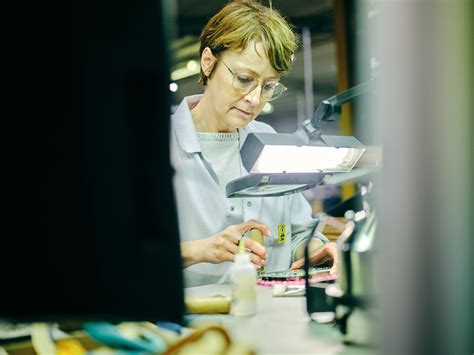
- Robust PCBA workflows integrate smart automation for tasks like paste dispensing and component soldering, minimizing human error in high-mix production.
| Challenge | Solution | Impact |
|---|---|---|
| Miniaturization demands | Embedded component technology | 40% space reduction in PCB assembly |
| Signal integrity issues | High-speed material substrates (e.g., Rogers 4350B) | Improved EMI shielding by 30% |
| Thermal management | Micro-via cooling structures | 25% lower operating temperatures |
Transitioning to these methodologies requires collaboration between design engineers and PCBA specialists to align electrical performance with manufacturability. By prioritizing scalable strategies, manufacturers can adapt to evolving requirements without compromising on yield rates or time-to-market. This foundation supports the subsequent exploration of precision techniques and reliability protocols in later sections.
Precision Techniques for Complex PCB Assembly
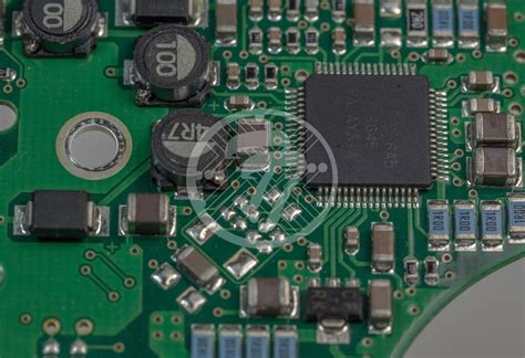
Modern PCB assembly processes demand meticulous attention to detail, particularly for high-density interconnects (HDIs) and multi-layered designs. Advanced PCBA workflows now incorporate laser-direct imaging (LDI) and automated optical inspection (AOI) to ensure micron-level accuracy in component placement. These methods address challenges like thermal management and signal integrity in compact layouts, where even minor misalignments can compromise performance.
"Implementing real-time monitoring systems during solder paste application reduces defects by up to 40%, according to industry studies."
For complex PCB assembly, manufacturers leverage 3D printing for rapid prototyping of intricate substrates, paired with embedded component technology to minimize footprint. High-precision pick-and-place machines, calibrated for 01005-sized components, enable reliable integration of micro-scale elements. Additionally, conformal coating techniques protect sensitive circuits from environmental stressors while maintaining electrical efficiency.
Tip: Prioritize design-for-manufacturing (DFM) checks early in the development cycle to identify potential assembly bottlenecks.
The shift toward ultra-fine-pitch BGAs and stacked via configurations further underscores the need for precision. By combining AI-driven defect detection with hybrid soldering processes, engineers achieve sub-10μm tolerances required for 5G and IoT applications. This synergy of innovation and exactitude ensures next-gen electronics meet escalating demands for speed, durability, and miniaturization.
Advanced Manufacturing Solutions for High-Density PCBs
Modern PCB assembly processes face escalating demands as next-generation electronics push the boundaries of miniaturization and performance. To address the intricate requirements of high-density interconnects (HDIs), manufacturers are adopting advanced manufacturing solutions that combine precision engineering with intelligent automation. Cutting-edge techniques like laser direct imaging (LDI) and microvia drilling enable the creation of ultra-fine traces and stacked vias, critical for compact PCBA designs. These methods ensure tighter tolerances—often below 25µm—while minimizing signal loss in densely packed layouts.
A key innovation lies in the integration of automated optical inspection (AOI) systems with machine learning algorithms. These systems detect microscopic defects in real time, such as solder bridging or misaligned components, which are common pain points in complex PCB assembly. Additionally, the use of low-temperature co-fired ceramics (LTCC) and advanced substrate materials enhances thermal management, a critical factor for high-power applications. By leveraging modular assembly lines, manufacturers achieve scalable production without compromising on the precision required for mixed-signal architectures.
Transitioning to these solutions not only accelerates time-to-market but also aligns with evolving industry standards for reliability and repeatability. As component densities continue to rise, the synergy between PCBA innovation and agile manufacturing frameworks becomes indispensable for meeting the exacting demands of aerospace, medical devices, and IoT ecosystems.
Optimizing PCB Integration in Next-Gen Electronics
Achieving seamless PCB assembly in next-generation electronics demands a holistic approach that balances component density, thermal management, and signal integrity. As devices shrink and performance requirements escalate, high-density interconnects (HDIs) and multilayer stacking have become critical for optimizing PCBA workflows. Advanced techniques like laser-drilled microvias and embedded passive components enable tighter integration while minimizing electromagnetic interference—a persistent challenge in complex PCB assembly.
To ensure precision, manufacturers are adopting adaptive placement algorithms and 3D solder paste inspection, which reduce defects in densely packed layouts. Material innovation also plays a pivotal role: high-frequency laminates and low-loss dielectrics maintain signal clarity in high-speed applications, from 5G modules to AI-driven hardware.
Automation further enhances consistency, with robotic pick-and-place systems handling micron-level tolerances for components like ball grid arrays (BGAs) and chip-scale packages. Real-time analytics integrated into PCBA lines allow for dynamic adjustments, ensuring yield rates remain above 98% even in high-mix production environments.
By aligning design-for-manufacturing (DFM) principles with scalable assembly processes, engineers can overcome the paradox of miniaturization without sacrificing reliability—a cornerstone for meeting the demands of next-gen electronics.
Overcoming Design Challenges in Compact PCB Assembly
Modern PCB assembly processes face escalating complexity as electronics shrink in size while expanding in functionality. Engineers must balance thermal management, signal integrity, and mechanical stability within increasingly confined spaces. High-density interconnect (HDI) designs, often essential for compact PCBA, require precision placement of microcomponents, which amplifies risks of solder bridging or misalignment. To address this, manufacturers employ laser-direct imaging (LDI) and automated optical inspection (AOI) systems to ensure sub-10µm accuracy during component placement.
Another critical hurdle lies in managing heat dissipation in tightly packed layouts. Advanced thermal vias and embedded cooling channels are integrated into multilayer boards to prevent overheating without compromising spatial efficiency. Additionally, impedance control becomes paramount in high-frequency applications, demanding meticulous trace routing and material selection to minimize signal loss.
Collaboration between design and manufacturing teams is vital. Leveraging design-for-manufacturability (DFM) principles early in the process reduces rework by aligning component footprints with PCB assembly capabilities. For instance, selecting low-voiding solder pastes or high-Tg substrates enhances reliability in miniaturized systems. By combining these strategies, manufacturers can navigate the intricate demands of compact PCBA while maintaining scalability for next-generation applications.
Ensuring Reliability in High-Performance PCB Systems
Achieving unwavering reliability in high-performance PCB systems demands rigorous attention to material selection, design validation, and manufacturing precision. As complex PCB assembly evolves to support next-gen electronics, engineers prioritize thermal management and signal integrity to prevent failures in demanding environments. Advanced PCBA processes now incorporate high-temperature laminates and copper-core substrates to dissipate heat effectively, particularly in applications requiring continuous operation under extreme conditions.
To mitigate risks in high-density PCB assembly, manufacturers employ automated optical inspection (AOI) and X-ray testing to detect micro-defects in solder joints or layer alignment. These quality assurance measures are critical for mission-critical applications like aerospace or medical devices, where component failure carries significant consequences. Additionally, implementing design-for-reliability (DFR) principles during prototyping ensures robust electrical connections and minimizes parasitic effects in multilayer designs.
Scalable testing protocols, including thermal cycling and vibration simulations, further validate PCB assembly durability. By adhering to IPC Class 3 standards for trace spacing and plating thickness, manufacturers guarantee compliance with industry benchmarks for high-performance systems. This multilayered approach—combining advanced materials, precision PCBA techniques, and exhaustive testing—forms the foundation for electronics that deliver consistent performance across their operational lifespan.
Smart Automation for Complex Circuit Board Assembly
The integration of smart automation into PCB assembly processes has become a cornerstone for addressing the intricate demands of modern electronics. Advanced robotic systems now handle high-density interconnects (HDIs) and microscopic component placements with sub-millimeter precision, eliminating human error in complex PCBA workflows. Machine vision-guided pick-and-place machines, for instance, achieve placement accuracies under 10µm, critical for miniaturized designs in IoT devices and wearables.
Automated optical inspection (AOI) systems further enhance quality control by scanning multi-layer PCBs for soldering defects or misalignments at speeds exceeding 500 components per minute. This real-time defect detection reduces rework cycles by up to 40%, accelerating time-to-market for high-performance electronics. Additionally, AI-driven process optimization tools analyze historical PCBA data to predict thermal stress points and recommend layout adjustments, ensuring reliability in extreme operating conditions.
By synchronizing automated assembly lines with digital twin simulations, manufacturers achieve end-to-end traceability while maintaining flexibility for design iterations. Such systems adapt seamlessly to mixed-batch production, a necessity for industries requiring both scalability and customization. As next-gen applications push the boundaries of PCB assembly complexity, smart automation remains indispensable for balancing precision, efficiency, and innovation.
Meeting Demands for Miniaturized Electronics via PCB Innovation
The relentless push for smaller, more powerful devices has driven transformative advancements in PCB assembly methodologies. Modern miniaturized electronics demand ultra-compact designs without compromising functionality, requiring PCBA processes to achieve unprecedented component density and precision. Innovations such as laser-direct imaging and microvia drilling enable the creation of intricate multilayer boards that support high-speed signal transmission in space-constrained applications.
To address thermal management challenges in dense layouts, engineers now leverage embedded passive components and advanced substrate materials, which reduce footprint while enhancing heat dissipation. Additionally, automated optical inspection (AOI) systems ensure microscopic alignment accuracy during PCB assembly, critical for maintaining reliability in wearables, medical implants, and IoT devices.
A key breakthrough lies in hybrid manufacturing approaches that combine traditional PCBA techniques with additive printing, allowing for flexible circuit geometries tailored to unconventional form factors. This synergy not only accelerates prototyping but also supports scalable production of high-density interconnects essential for 5G modules and AI-driven hardware.
As electronic devices shrink further, the integration of machine learning algorithms into design software helps predict and mitigate signal integrity risks early in the PCB assembly lifecycle. These innovations collectively position PCBA as the backbone of next-generation electronics, balancing miniaturization demands with uncompromised performance.
Scalable Strategies for Next-Level PCB Manufacturing
Achieving scalability in PCB assembly requires balancing precision with adaptable production frameworks. As next-generation electronics demand both miniaturization and multi-functional integration, manufacturers must adopt PCBA processes that seamlessly transition from prototyping to mass production. Modular design architectures enable this flexibility, allowing engineers to standardize core components while accommodating custom configurations for specialized applications. Implementing adaptive soldering techniques and dynamic thermal management systems ensures consistent quality across varying batch sizes, even when handling high-density interconnects or mixed-technology boards.
Advanced data analytics further enhance scalability by predicting bottlenecks in PCB assembly workflows, from component placement accuracy to post-production testing. For instance, machine learning algorithms optimize feeder setups in PCBA lines, reducing changeover times by up to 40% in multi-product environments. Pairing this with cloud-based inventory management systems creates a responsive supply chain capable of scaling production without compromising lead times. Crucially, these strategies maintain alignment with evolving industry standards, such as IPC-6012E for rigid boards or IPC-2226 for HDI designs, ensuring reliability remains uncompromised at every scale. By integrating these approaches, manufacturers can efficiently address both current and emerging requirements for high-performance electronics while future-proofing their PCB assembly capabilities.
Conclusion
The evolution of PCB assembly processes underscores the critical balance between precision engineering and scalable manufacturing in next-generation electronics. As high-density interconnects and multi-layer architectures dominate modern designs, PCBA workflows must prioritize material compatibility, thermal management, and signal integrity verification to maintain reliability. Advanced techniques like laser-drilled microvias and automated optical inspection (AOI) have become indispensable for addressing the geometric complexities of compact layouts while ensuring error-free PCB assembly.
To meet escalating demands for miniaturization, manufacturers are integrating machine learning-driven defect detection and adaptive placement algorithms into PCBA lines, reducing cycle times without compromising accuracy. These innovations, combined with high-frequency substrate materials and 3D-printed circuitry, enable seamless integration of heterogeneous components—a cornerstone for IoT devices and AI-driven systems.
Ultimately, the success of complex PCB assembly hinges on collaborative frameworks that bridge design intent with production realities. By adopting modular assembly strategies and real-time quality analytics, industries can future-proof their manufacturing ecosystems while delivering high-performance PCB systems that power tomorrow’s technological breakthroughs.
FAQs
What distinguishes complex PCB assembly from standard PCB manufacturing?
PCB assembly for advanced electronics requires handling high-density interconnects, multilayer stacking, and precision component placement. Unlike standard PCBA, it demands specialized equipment and expertise to manage tighter tolerances and advanced materials like high-frequency substrates.
How do manufacturers ensure reliability in miniaturized PCB designs?
Robust testing protocols, including automated optical inspection (AOI) and X-ray analysis, validate solder joint integrity and component alignment. Thermal management strategies, such as embedded heat sinks, are critical for high-performance PCB systems operating in demanding environments.
Can smart automation reduce errors in complex assemblies?
Yes. Automated pick-and-place systems and AI-driven inspection tools minimize human error while accelerating production. These technologies are vital for scaling PCB assembly processes without compromising precision, especially for next-gen applications like IoT and 5G devices.
What challenges arise when integrating mixed-technology components?
Combining surface-mount (SMT) and through-hole (THT) components on a single board requires careful planning. Hybrid PCBA workflows ensure proper soldering profiles and avoid cross-contamination during reflow processes, maintaining signal integrity in high-density layouts.
How do design-for-manufacturing (DFM) principles optimize complex assemblies?
DFM guidelines address manufacturability constraints early in the design phase, reducing rework. Techniques like panelization and standardized footprint libraries streamline PCB assembly, enabling faster turnaround for prototypes and mass production.
Explore Advanced PCB Assembly Solutions
Please click here to learn how our PCB assembly services tackle complex design challenges.