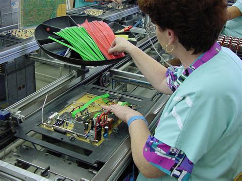
Streamlining Flex PCB Assembly for Modern Electronics Design
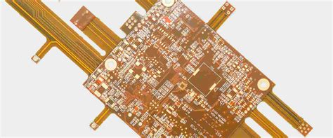
Key Takeaways
Optimizing flex PCB assembly processes is critical for meeting the demands of modern electronics, particularly in wearables and IoT devices. By integrating PCBA (Printed Circuit Board Assembly) automation, manufacturers achieve precision in component placement, reducing errors by up to 30% in high-density designs. Advanced techniques like laser drilling and automated optical inspection (AOI) ensure consistent quality, even in ultra-thin, flexible substrates.
"Designers should prioritize material compatibility early in the flex PCB development phase to avoid costly rework. Polyimide substrates, for example, offer superior thermal stability for compact IoT applications."
Cost efficiency is further enhanced through modular PCB assembly workflows, which minimize material waste and accelerate prototyping cycles. Innovations such as roll-to-roll processing enable scalable production of durable electronics, while standardized testing protocols reduce time-to-market by 20–40%. For wearable tech, dynamic bending endurance and moisture resistance are non-negotiable, driving adoption of hybrid rigid-flex PCBA solutions.
By balancing precision manufacturing with agile design practices, engineers can streamline flex PCB production without compromising reliability—a key advantage for industries prioritizing miniaturization and energy efficiency.
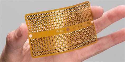
Optimizing Flex PCB Assembly
Achieving peak efficiency in flex PCB assembly requires balancing precision engineering with scalable production strategies. Unlike traditional rigid PCBA, flexible circuits demand specialized handling to maintain integrity during bending and folding cycles. Critical design factors such as material selection—polyimide substrates versus polyester films—directly impact thermal stability and signal reliability in compact devices.
Advanced PCB assembly techniques now incorporate automated optical inspection (AOI) systems to detect micro-fractures in traces, paired with laser-direct imaging (LDI) for sub-20μm alignment accuracy. These innovations reduce rework rates by 40–60% in high-density interconnects, a common requirement for wearables and IoT sensors.
To accelerate time-to-market, manufacturers are adopting panelization strategies that optimize board layouts for batch processing without compromising bend radii. Simultaneously, integrating PCBA testing protocols—like flying probe checks—ensures functional validation aligns with dynamic mechanical stress profiles. By standardizing component libraries for flex-specific footprints, designers can slash prototyping cycles by up to 30% while adhering to IPC-6013D standards.
The shift toward modular tooling and adaptive fixtures further streamlines transitions between prototype and mass production phases, a key advantage for IoT developers managing rapid iteration schedules. This approach not only enhances yield rates but also positions flex PCB assembly as a cost-competitive solution for next-gen electronics.
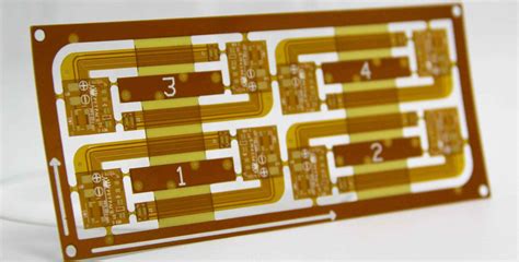
Precision in Flex PCB Manufacturing
Achieving micron-level accuracy in flex PCB assembly requires meticulous control over material selection, etching processes, and component placement. Modern high-density interconnect (HDI) technologies enable trace widths as narrow as 25μm, critical for compact wearables and IoT sensors. Advanced PCBA workflows leverage automated optical inspection (AOI) systems to detect defects like micro-cracks or misaligned solder joints, ensuring reliability in dynamic applications.
To maintain precision, manufacturers employ laser ablation for clean via formation and adopt polyimide substrates with low thermal expansion coefficients to withstand repeated bending. Embedded passives and rigid-flex designs further enhance signal integrity while minimizing spatial footprints. Real-time monitoring during PCB assembly reduces variability, particularly when handling ultra-thin copper layers (≤9μm). These innovations align with the growing demand for durable, high-performance electronics that operate seamlessly under mechanical stress.
By integrating adaptive stencil printing and 3D solder paste inspection (SPI), PCBA providers optimize yield rates without compromising on tolerances. Such precision-driven methodologies not only extend product lifespans but also pave the way for next-gen applications in medical implants and foldable displays.
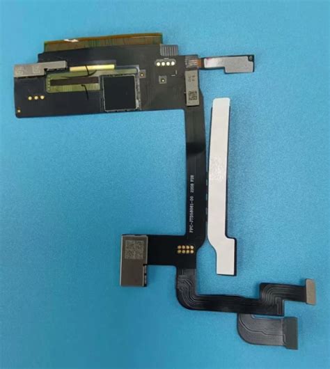
Cost-Effective Flex PCB for IoT
The proliferation of IoT devices demands flex PCB assembly solutions that balance performance and affordability. By optimizing PCBA processes, manufacturers can achieve significant cost reductions without compromising the reliability required for interconnected systems. A key strategy involves leveraging design-for-manufacturability (DFM) principles to minimize material waste and simplify assembly steps. For instance, selecting thinner polyimide substrates or adopting panelization techniques reduces raw material expenses while maintaining circuit integrity.
| Cost Factor | Traditional Approach | IoT-Optimized Approach |
|---|---|---|
| Material Utilization | Standard panel sizes | Customized nesting layouts |
| Assembly Automation | Limited to rigid boards | High-speed flex PCBA lines |
| Testing Efficiency | Manual inspections | Automated optical inspection |
Advanced laser drilling and direct imaging technologies further enhance precision in creating dense interconnects for compact IoT sensors. Additionally, partnering with PCB assembly providers that specialize in high-volume production ensures economies of scale, particularly for deployments requiring millions of units. To address thermal challenges in energy-efficient devices, engineers are integrating embedded passives directly into flexible circuits, eliminating the need for discrete components.
By aligning flex PCB design with IoT-specific requirements—such as low-power operation and environmental resilience—developers can achieve 30-40% cost savings compared to conventional rigid-flex hybrids. This approach not only accelerates time-to-market but also supports the scalability needed for next-generation smart infrastructure.
Advanced Flex PCB for Wearables
The integration of flex PCB assembly into wearable technology demands solutions that balance ultra-thin profiles with robust performance. Wearables, from fitness trackers to medical monitors, require circuits capable of conforming to dynamic shapes while maintaining signal integrity. Advanced PCBA techniques now leverage materials like polyimide substrates and adhesive-less laminates to achieve thicknesses below 0.2mm, enabling seamless integration into curved or stretchable designs.
To ensure reliability under constant motion, manufacturers employ laser-drilled microvias and high-density interconnects (HDI), which minimize space while maximizing electrical stability. These innovations are critical for devices subjected to dynamic bending cycles, such as smartwatches or biometric sensors. Additionally, automated optical inspection (AOI) systems paired with 3D solder paste inspection enhance precision in PCB assembly, reducing defects in components as small as 0201 packages.
For IoT-enabled wearables, low-power consumption and thermal management are prioritized. Embedded passive components and rigid-flex hybrid designs optimize energy efficiency, while copper-filled vias dissipate heat in compact layouts. By aligning PCBA workflows with wearables’ unique demands—such as moisture resistance and biocompatibility—developers accelerate time-to-market without compromising durability, ensuring next-generation devices meet both technical and user-experience expectations.
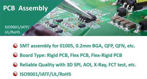
Accelerating Flex PCB Production
The drive to shorten flex PCB assembly timelines has become critical as demand surges for compact, high-performance electronics. Modern PCBA processes leverage automation and laser direct imaging (LDI) to slash turnaround times by up to 40%, enabling rapid prototyping and volume manufacturing. For instance, dynamic thermal profiling ensures precise solder paste curing during reflow, minimizing rework while maintaining signal integrity in ultra-thin substrates.
Advanced PCB assembly workflows now integrate AI-driven inspection systems, which reduce error rates by cross-referencing design files with real-time production data. This is particularly vital for applications like wearables, where component density and bend tolerance requirements are extreme. Additionally, modular production lines allow seamless switching between rigid-flex and pure flex designs, eliminating bottlenecks in mixed-product environments.
To further accelerate cycles, manufacturers are adopting just-in-time material sourcing paired with cloud-based collaboration platforms. These tools synchronize design iterations with PCBA readiness, cutting lead times from weeks to days. Such agility not only supports IoT device innovators in meeting tight launch deadlines but also ensures scalability as 5G and edge computing push the boundaries of flex PCB assembly complexity.
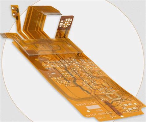
Streamlining Flex PCB Design
Efficient flex PCB design begins with optimizing layout geometries to match dynamic mechanical requirements while maintaining signal integrity. By adopting DFM (Design for Manufacturing) principles, engineers can reduce iterative revisions during PCB assembly, ensuring seamless integration with automated PCBA workflows. Critical factors like bend radius tolerance and component placement density directly influence manufacturability, particularly for high-frequency IoT or wearable applications.
Advanced simulation tools, such as 3D finite element analysis (FEA), enable precise modeling of flex circuits under stress, minimizing the risk of delamination or trace fractures post-assembly. Pairing these tools with standardized PCB assembly protocols ensures consistent quality across batches. Additionally, integrating laser-drilled microvias and adhesive-less base materials simplifies layer stacking, which accelerates prototyping and reduces PCBA lead times.
To further streamline processes, designers are leveraging AI-driven routing algorithms that balance electrical performance with thermal management needs. This approach not only enhances reliability but also cuts material waste by up to 20%, aligning with cost-reduction goals outlined in earlier sections. Collaboration between design and manufacturing teams remains pivotal, as early-stage adjustments in copper weight or stiffener placement can prevent costly rework during mass production.
Flex PCB Innovations for IoT
The rapid expansion of IoT ecosystems demands electronics that balance compact form factors with robust performance. Innovations in flex PCB assembly are addressing these needs by integrating high-density interconnects (HDIs) and multi-layer stacking techniques, enabling seamless integration into space-constrained sensors and edge devices. Advanced PCBA processes now leverage laser-direct imaging (LDI) to achieve micron-level accuracy, critical for maintaining signal integrity in low-power, high-frequency IoT applications.
A key breakthrough lies in the use of polyimide-based substrates with enhanced thermal stability, which withstand repeated bending cycles in wearable health monitors or industrial IoT nodes. Manufacturers are also adopting hybrid rigid-flex designs to reduce connector points, minimizing failure risks in harsh environments. For cost-sensitive IoT deployments, optimized PCB assembly workflows combine automated optical inspection (AOI) with AI-driven defect detection, slashing rework rates by up to 40%.
Transitioning toward scalable production, roll-to-roll (R2R) processing is accelerating the fabrication of ultra-thin flex circuits, while modular PCBA setups allow rapid customization for diverse IoT use cases. These advancements not only improve device longevity but also align with the IoT sector’s emphasis on energy efficiency—enabled by precision-etched conductive traces that minimize parasitic losses. As IoT networks grow denser, these innovations ensure flex PCB technologies remain at the forefront of reliable, mass-producible connectivity solutions.
Reducing Flex PCB Costs
Achieving cost efficiency in flex PCB assembly requires strategic optimization across design, material selection, and production workflows. By adopting design for manufacturability (DFM) principles, engineers can minimize material waste and simplify PCBA processes. For instance, optimizing panel layouts to maximize substrate utilization reduces raw material expenses by up to 20%. Additionally, selecting thinner polyimide films or low-cost adhesives—without compromising durability—lowers bill-of-materials (BOM) costs while maintaining performance for wearables and IoT devices.
Automation plays a pivotal role in cutting flex PCB costs. Advanced pick-and-place systems and reflow soldering techniques accelerate PCBA cycles, reducing labor-intensive steps. Collaborative partnerships with suppliers for bulk purchasing of flexible laminates or standardized components further drives down unit prices. For high-volume orders, manufacturers often leverage economies of scale, passing savings to OEMs.
Proactive testing protocols, such as automated optical inspection (AOI), prevent costly post-assembly defects. Early identification of issues like solder bridging or misaligned components ensures higher first-pass yields, minimizing rework expenses. By integrating these strategies, businesses can achieve a 15–30% reduction in flex PCB assembly costs, enabling competitive pricing for next-generation electronics.
Conclusion
As the electronics industry continues to prioritize miniaturization and durability, flex PCB assembly remains a cornerstone of innovation. The integration of advanced PCBA techniques ensures that modern devices—from wearables to IoT sensors—achieve unparalleled reliability while maintaining cost efficiency. By leveraging automated processes and precision engineering, manufacturers can address the growing demand for compact, high-performance electronics without compromising on quality.
The shift toward thin-film substrates and laser-drilled vias in flex PCB manufacturing has not only accelerated production timelines but also enhanced the mechanical stability of end products. Furthermore, the adoption of rigid-flex hybrid designs allows engineers to balance complexity and space constraints, particularly in applications requiring robust interconnects.
To sustain this momentum, continuous collaboration between design and PCB assembly teams is critical. Early-stage simulation tools and real-time quality monitoring systems, such as automated optical inspection (AOI), help mitigate risks during PCBA stages, ensuring seamless scalability. As industries push the boundaries of what’s possible, refining these methodologies will remain essential for delivering next-generation electronics that meet both technical and economic expectations.
FAQs
How does flex PCB assembly differ from rigid PCB processes?
PCB assembly for flexible circuits requires specialized handling to accommodate bending and folding. Unlike rigid boards, dynamic environments demand precise material selection and solder mask application to maintain integrity during repeated flexing.
What design factors impact PCBA costs in high-volume production?
Component density, layer count, and advanced testing protocols significantly affect expenses. Optimizing panel layouts and selecting automated PCBA workflows can reduce material waste by up to 30% in IoT device manufacturing.
Can flex circuits withstand harsh industrial conditions?
Yes, when paired with polyimide substrates and protective coatings, PCB assembly processes yield boards resistant to moisture, vibrations, and temperature fluctuations. Accelerated life testing ensures compliance with aerospace and medical durability standards.
How do miniaturization trends affect wearables manufacturing?
Ultra-thin flex circuits enable sub-1mm bend radii, critical for smartwatches and health monitors. Laser-drilled microvias in PCBA designs allow 40% smaller footprints while maintaining signal integrity in high-frequency applications.
What certifications ensure quality in flex PCB production?
ISO 9001 and IPC-6013 Class 3 certifications validate processes for high-reliability applications. Third-party audits of PCB assembly facilities guarantee adherence to contamination-control protocols essential for medical-grade electronics.
Ready to Optimize Your Flex PCB Assembly Process?
Explore tailored solutions for your project at https://www.andwinpcb.com/pcb-assembly/. For technical specifications or consultation requests, please click here.


