Streamlining Flexible PCB Assembly for Next-Gen Devices

Key Takeaways
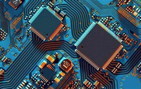
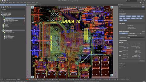
Modern PCB assembly processes for flexible circuits are revolutionizing how next-generation devices are manufactured. By integrating advanced PCBA techniques, engineers achieve unprecedented precision in handling ultrathin substrates and complex geometries. Key innovations include laser-direct imaging for micron-level accuracy and automated optical inspection (AOI) systems that ensure 99.98% defect-free output.
| Factor | Traditional PCBA | Flexible PCBA |
|---|---|---|
| Material Thickness | 1.6mm+ | 0.1–0.3mm |
| Bend Radius | Limited | ≤5mm |
| Assembly Yield | 92–95% | 97–99% |
The shift toward flexible PCB assembly directly addresses demands from wearables and IoT devices, where space constraints and dynamic form factors dominate. Manufacturers now prioritize roll-to-roll processing and conductive ink printing to reduce material waste by up to 40%, aligning with sustainability goals. Additionally, hybrid PCBA approaches combining rigid and flexible elements enable seamless integration in compact electronics like foldable displays.
To maintain cost-efficiency, suppliers leverage panelization strategies and modular tooling, cutting per-unit expenses by 15–25% without compromising reliability. These advancements underscore how optimized flexible PCB assembly is becoming the backbone of miniaturized, high-performance devices.

Next-Gen Flex PCB Assembly Innovations
The evolution of flexible PCB assembly is reshaping how next-generation electronics are designed and manufactured. Modern PCBA processes now integrate automated optical inspection (AOI) and laser direct imaging (LDI) to achieve micron-level precision in circuit patterning, essential for ultra-thin, bendable substrates. These advancements enable flexible PCBs to withstand repeated mechanical stress while maintaining signal integrity—a critical requirement for wearables and IoT devices.
Tip: To optimize yield rates in flexible PCB assembly, manufacturers should prioritize substrate material compatibility with high-temperature soldering processes, such as polyimide films paired with lead-free solder pastes.
Emerging techniques like 3D-printed circuitry and roll-to-roll manufacturing further streamline production, reducing material waste by up to 30%. The adoption of PCBA workflows with embedded component placement also minimizes footprint, aligning with the demand for compact electronics.
"The shift toward dynamic bend testing in quality control ensures reliability across 50,000+ flex cycles," notes Dr. Elena Torres, a materials engineer at FlexTech Alliance.
As manufacturers adopt these innovations, collaboration between designers and PCB assembly specialists becomes vital to balance performance, durability, and cost-efficiency. This synergy is particularly evident in medical wearables, where flexible PCBs must conform to ergonomic designs without compromising functionality.
Enhancing IoT Devices with Flexible Circuits
The rapid proliferation of IoT devices hinges on their ability to integrate seamlessly into space-constrained environments while maintaining robust functionality. Flexible circuits play a pivotal role here, offering unmatched adaptability for compact designs and irregular form factors. By leveraging advanced PCB assembly techniques, manufacturers can embed high-density interconnects into bendable substrates, ensuring reliable performance in wearables, environmental sensors, and smart home systems.
Modern PCBA workflows now prioritize precision alignment of components on flexible substrates, mitigating risks like signal loss or mechanical fatigue. For instance, automated optical inspection (AOI) systems verify solder joint integrity on dynamic flex circuits, which endure repeated bending in IoT applications. Additionally, the use of polyimide-based materials enhances thermal stability, allowing devices to operate efficiently in fluctuating temperatures—a critical requirement for outdoor or industrial IoT deployments.
Transitioning from rigid to flexible PCB assembly also reduces overall system weight and material waste, aligning with sustainability goals. This shift enables IoT developers to balance miniaturization with extended battery life, addressing two key consumer demands. As IoT networks expand, optimized PCBA processes for flexible circuits will remain central to delivering durable, high-performance devices capable of thriving in real-world conditions.
Precision Techniques in Flex PCB Manufacturing
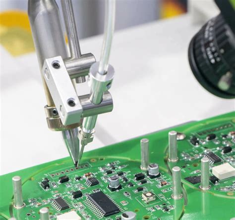
Achieving high-quality PCB assembly for flexible circuits demands meticulous attention to detail throughout the manufacturing process. Advanced PCBA workflows now integrate laser direct imaging (LDI) to ensure micron-level accuracy in etching conductive traces, critical for maintaining signal integrity in ultra-thin substrates. Automated optical inspection (AOI) systems further enhance precision by detecting defects as small as 10µm, reducing error rates in wearables and IoT devices where space constraints leave no margin for flaws.
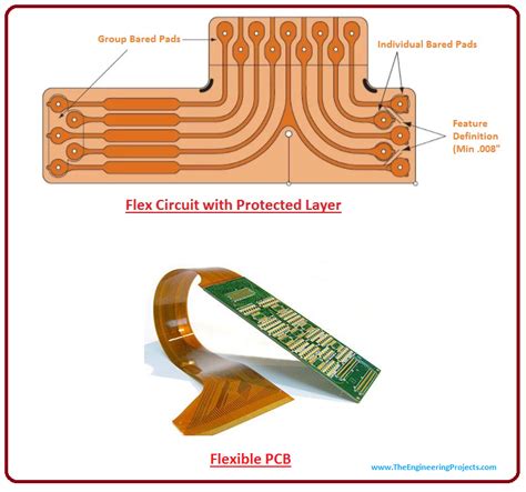
Material selection plays an equally vital role, with polyimide films and adhesiveless laminates offering superior thermal stability and bend endurance. Manufacturers employ controlled impedance testing to validate signal performance in dynamic applications, such as foldable displays or medical sensors. For flexible PCB assembly, sequential lamination techniques ensure layer alignment within ±25µm tolerances, even across multi-layer designs.
To address scalability challenges, robotic pick-and-place systems optimize component mounting on curved or irregular surfaces, while conductive ink printing enables seamless integration of antennas or sensors. These innovations not only streamline PCBA processes but also align with the growing demand for cost-efficiency without compromising reliability in next-gen electronics. As device miniaturization accelerates, these precision-driven methodologies remain central to delivering robust, high-performance flexible circuits.
Cost-Effective Assembly for Flexible PCBs
Achieving cost efficiency in flexible PCB assembly requires balancing advanced manufacturing techniques with strategic material and process optimization. Unlike rigid boards, flexible circuits demand specialized handling during PCBA to prevent damage to delicate substrates like polyimide. Manufacturers leverage automated optical inspection (AOI) and precision pick-and-place systems to minimize errors, reducing rework costs while maintaining high yields. Additionally, design-for-manufacturability (DFM) principles play a critical role in streamlining workflows—optimizing panel layouts and minimizing material waste can lower production expenses by up to 20%.
The adoption of surface-mount technology (SMT) tailored for flexible substrates further enhances affordability. By using ultra-thin solder pastes and low-temperature curing adhesives, assemblers ensure reliable component attachment without compromising the integrity of bendable layers. For high-volume orders, economies of scale significantly reduce per-unit costs, making flexible PCB assembly viable for budget-sensitive applications like consumer wearables and IoT sensors. However, cost-cutting measures must align with quality standards; partnering with PCBA providers certified in IPC-6013 ensures durability even under repeated flexing.
Transitioning to cost-effective solutions does not mean sacrificing innovation. Integrating modular designs and standardized connectors simplifies assembly, while advanced simulation tools predict mechanical stress points early in development—preventing costly redesigns. This approach not only aligns with the broader focus on precision and reliability but also supports scalable production for next-generation devices.
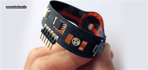
Wearable Technology Demands Flexible PCBs
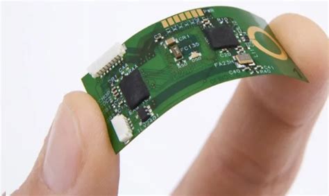
The rise of wearable technology—from fitness trackers to medical monitoring devices—has intensified the need for PCB assembly solutions that prioritize lightweight, durable, and adaptable designs. Unlike rigid boards, flexible PCBs conform to compact, irregular shapes while maintaining electrical integrity, making them indispensable for wearables that require seamless integration with the human body. Advanced PCBA processes now incorporate ultra-thin substrates and high-density interconnects, enabling circuits to withstand repeated bending and environmental stressors like moisture or temperature fluctuations.
For instance, smartwatches and health sensors rely on flexible PCB assembly to balance performance with ergonomics, ensuring uninterrupted data transmission even during dynamic movement. Manufacturers are also adopting laser-drilled microvias and automated optical inspection (AOI) to enhance precision in these miniature layouts. As consumer expectations shift toward sleeker, longer-lasting devices, optimizing flexible PCBA workflows becomes critical to reducing material waste and accelerating time-to-market. This alignment between design flexibility and manufacturing efficiency not only meets current wearable demands but also paves the way for innovations in next-gen medical wearables and augmented reality gadgets.
Compact Electronics Rely on Flex PCB Solutions
As consumer demand shifts toward smaller, lighter devices, flexible PCB assembly (flex PCBA) has become indispensable for compact electronics. The ultrathin, bendable nature of flexible circuits enables seamless integration into tight spaces, such as smartwatch components, medical implants, and miniature sensors. Unlike rigid boards, flex PCBs adapt to complex geometries, eliminating bulky connectors and reducing overall weight—a critical advantage for portable gadgets.
Modern PCB assembly processes leverage automated optical inspection (AOI) and laser direct imaging (LDI) to ensure micron-level accuracy in circuitry patterning. This precision is vital for maintaining signal integrity in high-density designs, where even minor misalignments can compromise performance. Additionally, advancements in thermoforming adhesives and conductive inks enhance durability, allowing flex circuits to withstand repeated bending cycles without failure.
For manufacturers, optimizing flexible PCBA workflows reduces material waste and accelerates time-to-market. Techniques like panelization with dynamic routing maximize yield, while roll-to-roll processing supports scalable production. By aligning design-for-manufacturability (DFM) principles with flex PCB capabilities, engineers achieve cost-efficiency without sacrificing reliability—key for meeting the stringent demands of next-generation compact electronics.
Ensuring Reliability in Flexible PCB Production
Achieving consistent reliability in flexible PCB assembly requires meticulous attention to material selection, manufacturing processes, and testing protocols. Unlike rigid boards, flexible circuits demand substrates and conductive materials that withstand repeated bending without compromising electrical integrity. Advanced PCBA workflows now incorporate polyimide films and adhesives optimized for thermal stability, ensuring performance in high-stress environments like wearables or automotive electronics.
Critical to reliability is the implementation of automated optical inspection (AOI) systems, which detect micro-cracks or misalignments imperceptible to the human eye. Additionally, controlled impedance testing validates signal integrity in high-frequency applications common to IoT devices. Manufacturers are increasingly adopting laser-direct imaging (LDI) for precise trace patterning, minimizing errors that could lead to field failures.
Environmental stressors, such as humidity and temperature fluctuations, further necessitate conformal coatings tailored for flexible PCB assembly. These coatings protect against corrosion while maintaining the board’s pliability. By integrating failure mode and effects analysis (FMEA) during design phases, engineers preemptively address risks, aligning with industry standards like IPC-6013 for flexible circuits.
As next-gen devices push miniaturization limits, the interplay between PCBA precision and material innovation becomes paramount—ensuring that flexibility never comes at the cost of durability.
Advanced Methods for Streamlined PCB Assembly
Modern PCB assembly workflows leverage cutting-edge technologies to address the growing complexity of flexible circuit integration. Automated optical inspection (AOI) systems now incorporate machine learning algorithms to detect micron-level defects in flexible PCBs, ensuring compliance with stringent quality standards for wearables and IoT devices. Robotic pick-and-place machines equipped with vision-guided alignment achieve placement accuracies under 15µm, critical for high-density interconnects in compact electronics.
The adoption of laser direct imaging (LDI) eliminates photomasks in PCBA processes, reducing production lead times by 40% while maintaining ±5µm trace width consistency. Manufacturers are integrating PCB assembly lines with real-time thermal profiling systems, dynamically adjusting reflow parameters to prevent warping in heat-sensitive polyimide substrates.
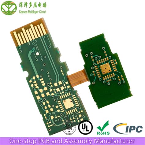
For hybrid rigid-flex designs, sequential lamination techniques combined with 3D modeling software enable precise layer registration across multiple bending zones. This approach minimizes material waste during flexible PCB fabrication while ensuring mechanical durability across 100,000+ flex cycles. Advanced design-for-manufacturing (DFM) protocols now automate via placement optimization, balancing signal integrity requirements with assembly feasibility in next-gen medical sensors and foldable displays.
Transitioning to these methods requires synchronized collaboration between PCBA engineers and material scientists, particularly when working with stretchable conductive inks or ultra-thin dielectric layers below 25µm. Such innovations collectively address the dual challenges of scalability and precision in flexible circuit manufacturing.
Conclusion
The evolution of flexible PCB assembly has become a cornerstone in developing next-generation electronics, balancing precision, durability, and scalability. As industries demand thinner, lighter, and more resilient devices, PCBA processes must adapt to accommodate complex geometries and dynamic applications. Advanced techniques like laser-direct imaging and automated component placement now enable tighter tolerances for flexible circuits, critical for wearables and IoT systems where space constraints are paramount.
Cost-efficiency remains a driving factor, with optimized material selection and modular PCB assembly workflows reducing waste while maintaining signal integrity. Manufacturers leveraging roll-to-roll processing and in-line testing further enhance yield rates, ensuring reliability across high-volume production. For compact electronics and medical devices, this translates to repeatable performance under mechanical stress or environmental extremes.
Looking ahead, the integration of AI-driven defect detection and hybrid rigid-flex designs will push boundaries in flexible PCB innovation. By aligning PCBA strategies with emerging material science, engineers can unlock new possibilities for foldable displays, biodegradable substrates, and ultra-low-power IoT nodes. The future of electronics hinges on refining these assembly paradigms to meet both technical and economic demands—without compromising the agility that defines modern device ecosystems.

FAQs
How does flexible PCB assembly differ from rigid PCB processes?
PCB assembly for flexible circuits requires specialized handling of polyimide substrates and dynamic bending environments. Unlike rigid PCBA, processes involve lower-temperature soldering and strain-relief designs to maintain circuit integrity during repeated flexing.
What design considerations optimize flexible PCBA reliability?
Critical factors include trace spacing adjustments, proper adhesive selection, and strategic stiffener placement. Advanced PCB assembly techniques like laser-cut apertures and automated optical inspection (AOI) ensure precision in high-density layouts.
Can flexible circuits match the cost-efficiency of rigid PCBs?
While initial PCBA costs may be higher, flexible designs reduce long-term expenses by eliminating connectors and enabling compact form factors. Volume production and panelization strategies further enhance cost-effectiveness for wearables and IoT devices.
How do thermal management practices vary in flexible PCB assembly?
Thin, thermally conductive materials like adhesive-less laminates dissipate heat efficiently. Engineers often integrate copper-filled vias or hybrid rigid-flex designs to manage thermal stress in high-power applications.
What industries benefit most from advanced flexible PCBA?
Beyond consumer electronics, sectors like medical implants, aerospace avionics, and automotive sensors leverage flexible circuits for their durability in vibration-prone environments and space-constrained configurations.
Ready to Optimize Your Flexible PCB Assembly?
For expert PCB assembly solutions tailored to next-gen devices, please click here to explore advanced PCBA capabilities that ensure performance and scalability.