Streamlining Multilayer PCB Assembly for High-Density Circuitry
Key Takeaways
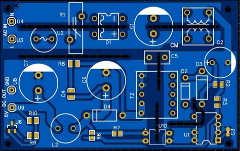
Effective multilayer PCB assembly requires a combination of precision engineering and advanced manufacturing methodologies to address the demands of high-density circuitry. Key considerations include leveraging automated optical inspection (AOI) and X-ray inspection to ensure layer alignment accuracy, which is critical for minimizing signal loss in PCBA designs. Additionally, optimizing thermal management through material selection and controlled impedance routing helps maintain reliability in complex, densely packed boards.
For cost efficiency, integrating design-for-manufacturing (DFM) principles early in the PCB assembly process reduces rework risks, while advanced stackup configurations enhance signal integrity. Manufacturers also prioritize laser-drilled microvias and sequential lamination techniques to support intricate interconnects without compromising structural stability. By adopting these strategies, PCBA providers can balance performance, scalability, and production timelines for next-generation electronics.
Transitioning to streamlined workflows further involves harmonizing surface-mount technology (SMT) with mixed-technology assemblies, ensuring compatibility across diverse component types. This holistic approach addresses both technical and economic challenges inherent in multilayer PCB assembly, positioning teams to meet evolving industry standards efficiently.
Advanced PCB Assembly Techniques
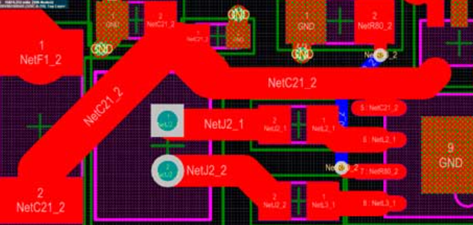
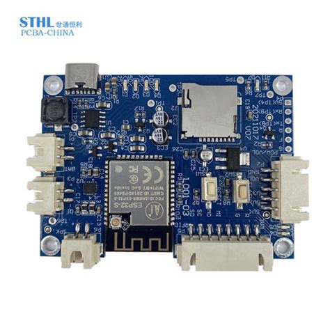
Modern PCB assembly processes demand sophisticated approaches to address the complexities of high-density circuitry. PCBA (Printed Circuit Board Assembly) for multilayer designs requires precise alignment of components, optimized thermal management, and meticulous soldering techniques. Advanced methods such as laser-direct imaging (LDI) and automated optical inspection (AOI) ensure accuracy in trace routing and component placement, particularly for boards with 8+ layers.
Tip: Implement sequential lamination during PCB assembly to minimize signal loss in high-speed applications. This technique helps maintain impedance control across multilayer stacks.
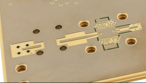
The integration of high-density interconnect (HDI) technology enables tighter via spacing and microvia drilling, critical for compact layouts. Additionally, surface-mount technology (SMT) advancements allow for finer-pitch components, reducing footprint while enhancing electrical performance. For PCBA reliability, manufacturers now leverage nitrogen-reflow soldering to minimize oxidation risks in dense circuit clusters.
Material selection also plays a pivotal role. High-Tg (glass transition temperature) substrates and low-loss dielectrics improve thermal stability, especially in via-in-pad configurations common in multilayer boards. Combining these with real-time process monitoring systems ensures consistent quality across high-volume production runs.
Designers should prioritize DFM (Design for Manufacturing) checks early in the PCB assembly workflow to avoid costly rework. Tools like 3D modeling software can identify potential conflicts in component placement or layer alignment.
By adopting these advanced techniques, manufacturers achieve a balance between precision, scalability, and cost-efficiency—key factors for delivering robust PCBA solutions tailored to high-density applications.
Efficient High-Density Circuit Assembly
Achieving efficient high-density circuit assembly demands a meticulous integration of design, material selection, and PCB assembly workflows. Modern high-density interconnect (HDI) designs rely on PCBA processes that balance precision with scalability, particularly when handling intricate multilayer layouts. Advanced techniques such as laser-drilled microvias and sequential lamination enable tighter component placement while minimizing signal loss, critical for applications like 5G infrastructure or IoT devices.
To optimize throughput, manufacturers prioritize automated optical inspection (AOI) systems and design-for-manufacturability (DFM) checks during PCB assembly, ensuring alignment with tolerances as low as 2/2 mil. The use of low-temperature co-fired ceramics (LTCC) and high-performance substrates further enhances thermal stability in densely packed circuits. However, challenges like solder bridging in PCBA require precise reflow profiles and nitrogen-assisted soldering to maintain yield rates above 98%.
Transitioning to streamlined workflows, many providers now adopt modular PCB assembly lines capable of rapid reconfiguration for mixed-batch production. This approach reduces lead times by 20–30% while maintaining compliance with IPC-6012 Class 3 standards. By harmonizing these strategies, engineers can address the growing demand for compact, high-reliability electronics without compromising on cost or performance.
Precision Multilayer Board Manufacturing
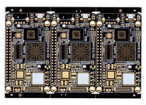
At the core of high-performance electronics lies multilayer PCB assembly, where precision manufacturing ensures seamless integration of complex circuitry. Modern PCBA processes employ laser direct imaging (LDI) and automated optical inspection (AOI) to achieve tolerances below 25µm, critical for high-density interconnects (HDIs) in applications like 5G modules and IoT devices. Advanced lamination techniques, combined with sequential build-up (SBU) methods, enable consistent layer alignment while minimizing signal loss across 12+ layer stacks.
Material selection plays a pivotal role, with low-loss dielectrics and high-Tg laminates becoming standard for thermal stability in PCB assembly. Manufacturers leverage impedance-controlled routing and microvia technologies to maintain signal integrity, particularly in mixed-signal designs. To address warpage risks in ultrathin cores, stress-testing protocols and dynamic thermal profiling are integrated into production workflows.
This approach not only enhances yield rates but also aligns with the broader goal of streamlined PCBA for dense layouts. By incorporating design-for-manufacturing (DFM) principles early in the process, engineers mitigate issues like copper imbalance or via cracking. The result is a manufacturing framework where precision meets scalability, directly supporting the reliability demands of aerospace, medical, and automotive systems.
Optimizing Reliability in Complex PCBs
Ensuring long-term reliability in multilayer PCB assembly demands meticulous attention to material selection, thermal management, and signal integrity. As circuit density increases, challenges like thermal stress and cross-talk interference become critical factors affecting performance. Advanced PCBA processes now integrate precision-controlled soldering techniques, such as laser reflow and vacuum-assisted bonding, to minimize voids and ensure robust interlayer connections.
Material compatibility plays a pivotal role, with high-glass transition temperature (Tg) laminates and low-loss dielectrics becoming standard for high-density designs. Additionally, automated optical inspection (AOI) and X-ray tomography are employed to detect micro-defects in PCB assembly layers that traditional methods might overlook. For mission-critical applications, sequential lamination strategies combined with via-in-pad structures enhance mechanical stability while reducing impedance mismatches.
To mitigate risks in complex layouts, designers prioritize symmetrical stackup configurations and balanced copper distribution, which prevent warping during thermal cycling. Rigorous testing protocols, including thermal shock and accelerated life testing, validate the durability of multilayer PCBA under extreme conditions. By aligning design intent with manufacturing capabilities, engineers achieve repeatable quality without compromising scalability—a cornerstone for next-generation electronics requiring uncompromised reliability.
Cost-Effective Multilayer PCB Strategies
Achieving affordability in multilayer PCB assembly requires balancing advanced techniques with strategic resource allocation. A primary focus lies in optimizing design-for-manufacturing (DFM) principles to minimize material waste and reduce rework. By integrating automated optical inspection (AOI) early in the PCBA process, manufacturers can identify defects at initial stages, lowering long-term corrective costs. Additionally, leveraging standardized layer stackups and panelization strategies enhances yield rates, particularly for high-density designs.
| Strategy | Cost Impact (%) | Key Benefit |
|---|---|---|
| DFM Optimization | 15–25 | Reduces material waste |
| Panelization Efficiency | 10–20 | Maximizes substrate utilization |
| Automated Testing | 12–18 | Lowers defect escape rates |
Collaborating with suppliers to source cost-effective, yet reliable, laminates and prepregs further drives down expenses without compromising performance. For instance, substituting high-frequency materials with cost-optimized alternatives in non-critical layers can reduce bill-of-materials (BOM) costs by up to 30%. Similarly, adopting modular PCB assembly workflows allows reuse of proven subassemblies across projects, accelerating time-to-market.
Transitioning to volume-based pricing models for PCBA services, combined with predictive maintenance of assembly equipment, ensures sustained cost efficiency. This approach not only aligns with the demands of high-density circuitry but also supports scalability for evolving production needs. By prioritizing these strategies, manufacturers can deliver robust multilayer solutions that meet both technical and budgetary requirements.
Overcoming High-Density Design Challenges
Modern electronics’ push for miniaturization and enhanced functionality has intensified the complexities of PCB assembly for high-density circuitry. As component densities increase, engineers face critical hurdles such as thermal management, signal integrity preservation, and maintaining adequate spacing between traces. Advanced manufacturing techniques like laser-drilled microvias and high-precision solder paste stenciling are now essential to address these challenges. For PCBA projects involving multilayer boards, optimizing layer stackup configurations becomes pivotal—ensuring proper grounding, reducing electromagnetic interference (EMI), and accommodating high-speed signals.
To mitigate risks in dense layouts, designers leverage sequential lamination processes and high-density interconnect (HDI) substrates, which enable tighter trace widths and finer pitch components. However, these solutions demand rigorous design-for-manufacturing (DFM) checks to avoid defects like solder bridging or delamination. Automated optical inspection (AOI) and X-ray testing further enhance quality control, particularly for hidden vias and buried components.
Balancing performance with manufacturability requires collaboration between design and PCB assembly teams. Strategies such as incorporating thermal relief pads and impedance-controlled routing ensure reliability without compromising space efficiency. By integrating these approaches, PCBA workflows achieve robust outcomes even in the most demanding high-density applications.
Innovative Stackup Solutions for PCBs
Effective PCB assembly relies heavily on strategic stackup design, particularly for high-density circuitry requiring precision and reliability. By optimizing layer arrangements, engineers can mitigate electromagnetic interference (EMI), reduce crosstalk, and enhance signal integrity in multilayer PCB assembly. Advanced stackup configurations often incorporate hybrid materials, such as high-Tg laminates paired with low-loss dielectrics, to balance thermal stability and electrical performance. For instance, alternating power and ground planes within the stackup minimizes impedance variations, a critical factor in high-speed applications.
To further streamline PCBA workflows, designers leverage simulation tools to model heat dissipation and signal behavior across layers. This proactive approach ensures that complex designs meet stringent manufacturing tolerances while avoiding costly rework. Additionally, integrating microvia technology and sequential lamination processes enables tighter interlayer connections, essential for compact, high-layer-count boards. Such innovations not only improve yield rates but also align with cost-effective multilayer PCB strategies, ensuring scalability for mass production.
By prioritizing stackup flexibility and material compatibility, manufacturers can address evolving demands for miniaturization without compromising durability. This alignment between design and PCB assembly processes underscores the importance of collaboration between engineering and fabrication teams to achieve repeatable success in high-density circuit applications.
Streamlined Processes for Dense Circuitry
Modern PCB assembly workflows for high-density designs demand precision-driven methodologies to manage intricate layouts and tight tolerances. PCBA (Printed Circuit Board Assembly) specialists achieve this by integrating automated optical inspection (AOI) systems, laser-drilled microvias, and sequential lamination techniques. These advancements enable precise alignment of multilayer interconnects, reducing signal loss and crosstalk in densely packed circuits.
A critical focus lies in optimizing solder paste application through stencil printing innovations, such as step-down apertures, which improve deposition accuracy for 0201 or 0.4mm pitch components. Concurrently, reflow profiling tailored to mixed-technology boards—combining BGAs, QFNs, and fine-pitch ICs—ensures consistent joint formation without thermal stress. Advanced design-for-manufacturing (DFM) checks further streamline workflows by preempting issues like copper imbalance or via starvation in complex stackups.
To enhance scalability, manufacturers adopt modular PCB assembly lines with real-time process monitoring. This allows rapid adjustments for high-mix production while maintaining IPC Class 3 standards. By balancing speed and precision, PCBA providers deliver robust solutions for applications ranging from aerospace avionics to miniaturized IoT devices, where reliability under extreme conditions is non-negotiable.
Conclusion
As modern electronics demand increasingly compact yet powerful solutions, multilayer PCB assembly emerges as a cornerstone for achieving high-density circuitry without compromising performance. By integrating PCBA methodologies with advanced manufacturing protocols, engineers can address challenges like signal integrity and thermal management in complex designs. The adoption of precision laser drilling, automated optical inspection (AOI), and controlled impedance routing ensures that PCB assembly processes meet stringent reliability standards while minimizing production errors.
For industries relying on mission-critical applications, optimizing multilayer PCB stackups and material selection remains pivotal. Pairing robust design validation tools with scalable fabrication workflows not only accelerates time-to-market but also reduces long-term costs associated with rework or field failures. As innovations in embedded components and hybrid materials continue to evolve, the synergy between PCBA expertise and cutting-edge technology will further redefine the boundaries of what’s achievable in high-density electronic systems. This progression underscores the importance of aligning engineering foresight with manufacturing precision to sustain competitiveness in an era defined by miniaturization and functional complexity.
Frequently Asked Questions
What are the key challenges in high-density PCB assembly?
High-density PCB assembly requires managing tighter trace spacing, microvia placement, and thermal dissipation. Advanced PCBA techniques, such as laser drilling and sequential lamination, address these challenges while maintaining signal integrity in complex multilayer designs.
How does stackup configuration impact multilayer PCB reliability?
A well-designed stackup balances impedance control, heat distribution, and mechanical stability. Proper material selection and layer alignment during multilayer PCB assembly minimize crosstalk and delamination risks, ensuring long-term performance in demanding applications.
What strategies reduce costs in high-volume PCBA projects?
Optimizing panel utilization, automating solder paste inspection (SPI), and adopting design-for-manufacturability (DFM) principles streamline PCBA workflows. Bulk material procurement and standardized testing protocols further enhance cost efficiency without compromising quality.
How are signal integrity issues mitigated in dense circuitry?
Controlled impedance routing, ground plane optimization, and advanced simulation tools are critical. Manufacturers often employ embedded passive components and hybrid stackups during multilayer PCB assembly to reduce electromagnetic interference (EMI) in high-speed designs.
Explore Custom Multilayer PCB Solutions Today
For tailored guidance on optimizing your PCB assembly process, please click here to connect with our engineering team. Discover how advanced PCBA methodologies can elevate your high-density circuitry projects.