Streamlining PCB Assembly: Component Integration Methods
Key Takeaways
Effective PCB assembly relies on strategic component integration to balance performance, cost, and reliability. Central to this process is optimizing PCBA layouts through automated systems, which minimize human error while accelerating production. Key strategies include:
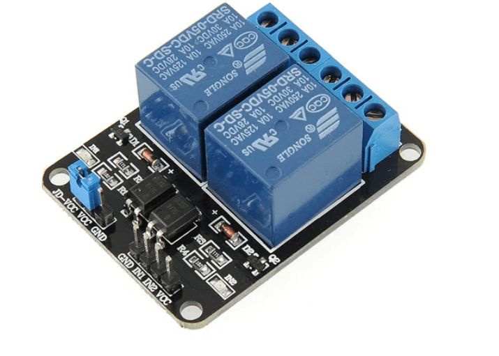
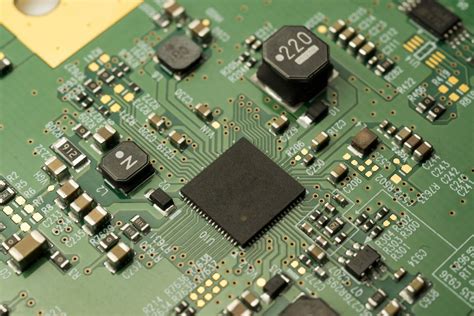
- Surface-mount technology (SMT) for compact, high-density designs, reducing manual soldering and improving signal integrity.
- Precision placement algorithms that align components with millimeter-level accuracy, critical for complex circuits.
- Rigorous thermal management practices to prevent overheating in densely packed boards.
"Integrating automated optical inspection (AOI) systems ensures 99.9% defect detection rates, safeguarding PCB assembly quality before final testing."
Modern PCBA workflows also leverage modular design principles, allowing reusable subassemblies to cut development time. For cost-sensitive projects, combining surface-mount devices (SMDs) with selective automation strikes a balance between scalability and affordability.
Tip: Prioritize component grouping by function during layout planning to simplify trace routing and minimize cross-interference.
Adopting predictive maintenance for assembly machinery further reduces downtime, while real-time analytics refine process parameters. These methods collectively enhance PCB assembly reliability, ensuring compliance with industry standards like IPC-A-610. By aligning integration techniques with automated systems, manufacturers achieve faster time-to-market without compromising on precision.
PCB Component Integration Strategies
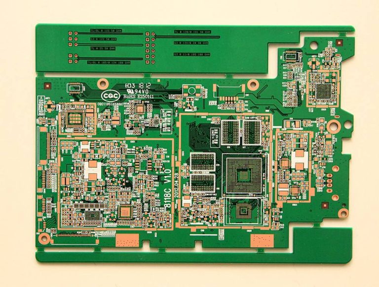
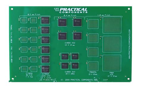
Effective PCB assembly relies on strategic component integration to balance performance, manufacturability, and cost. A critical first step involves grouping components by function, such as separating analog and digital circuits to minimize interference. This approach not only simplifies routing but also enhances signal integrity. Designers often prioritize surface-mount technology (SMT) for compact layouts, as its smaller footprints enable higher component density compared to traditional through-hole methods.
| Integration Method | Key Benefit | Common Use Case |
|---|---|---|
| SMT | Space efficiency | High-density PCBA designs |
| Through-Hole | Mechanical stability | Heavy components or connectors |
| Mixed Technology | Flexibility in complex layouts | Hybrid industrial systems |
Automated PCB assembly systems further refine integration by leveraging machine vision and precision robotics to place components within micrometer-level accuracy. This reduces human error and accelerates throughput, particularly in high-volume production. Thermal management also plays a role—strategic placement of heat-generating components near cooling features (e.g., vias or heatsinks) prevents overheating without compromising layout efficiency.
By aligning integration strategies with PCBA design rules, manufacturers achieve shorter lead times, lower material waste, and improved reliability—key factors in competitive electronics markets.
Efficient PCB Assembly Placement Methods
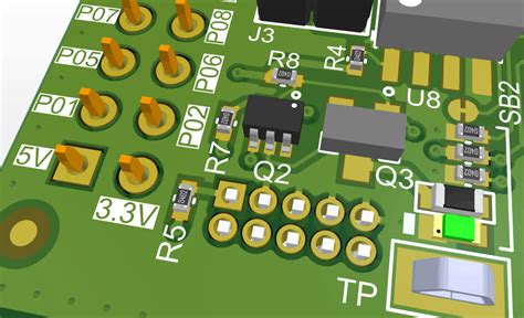
Effective PCB assembly relies on precise component placement strategies to minimize errors and maximize performance. By implementing design-for-manufacturing (DFM) principles, engineers can optimize the arrangement of components assembled on PCBs, ensuring alignment with automated assembly workflows. For instance, grouping similar components—such as resistors or capacitors—into logical clusters reduces machine movement during PCBA, accelerating production cycles.
A critical consideration is balancing thermal management with signal integrity. High-power components, like voltage regulators, should be positioned to avoid heat concentration, while sensitive analog circuits require isolation from digital noise sources. Advanced software tools simulate placement efficiency, identifying potential interference or routing bottlenecks before physical assembly begins.
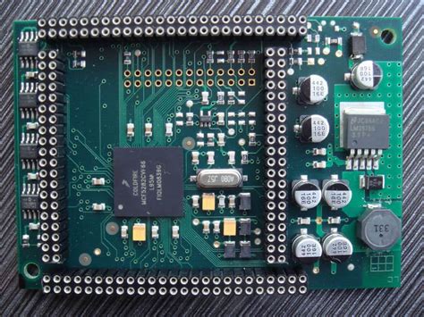
Additionally, adopting standardized footprints for surface-mount devices (SMDs) streamlines compatibility with pick-and-place systems. This approach not only reduces manual adjustments but also enhances repeatability across batches. For mixed-technology boards, combining through-hole and SMD components demands strategic zoning to prevent soldering conflicts.
Finally, incorporating automated optical inspection (AOI) checkpoints validates placement accuracy post-assembly, catching misalignments early. These methodologies collectively ensure that PCB assembly processes remain scalable, cost-effective, and aligned with modern manufacturing demands.
Surface-Mount Technology for Streamlined PCBs
In contrast to traditional through-hole methods, surface-mount technology (SMT) has revolutionized PCB assembly by enabling higher component density and faster production cycles. By mounting components directly onto the board’s surface, SMT eliminates the need for drilled holes, reducing material waste and simplifying the PCBA process. This approach supports miniaturization trends, allowing designers to place smaller, lighter components closer together without compromising electrical performance.
Advanced SMT systems utilize automated pick-and-place machines to position components with micron-level precision, significantly lowering the risk of human error. The use of reflow soldering further enhances reliability, as it ensures uniform thermal distribution across solder joints, minimizing defects like cold joints or bridging. Additionally, SMT-compatible components—such as chip resistors and quad flat packages—are optimized for high-speed placement, making them ideal for high-volume PCB assembly workflows.
A key advantage of SMT lies in its compatibility with mixed-technology boards, where surface-mount and through-hole components coexist. This flexibility supports iterative design improvements while maintaining cost efficiency. By integrating SMT into PCBA workflows, manufacturers achieve faster turnaround times and improved scalability, paving the way for more robust automation in subsequent production stages.
Automated Systems Reducing Assembly Errors
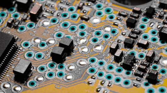
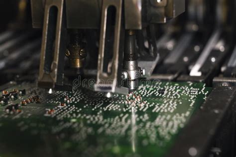
The adoption of automated systems in PCB assembly has revolutionized error reduction by minimizing human intervention in critical processes. Advanced pick-and-place machines, guided by precision algorithms, ensure components are positioned with micron-level accuracy, significantly lowering misalignment risks. These systems integrate real-time optical inspection (AOI) to detect flaws such as solder bridging or misplaced parts before they escalate into costly defects. By leveraging PCBA (printed circuit board assembly) automation, manufacturers achieve repeatable consistency across high-volume production runs—a stark contrast to manual methods prone to variability.
Moreover, automated workflows synchronize with design files to validate component orientation and polarity, virtually eliminating errors caused by misinterpretation of schematics. Closed-loop feedback mechanisms further refine processes by analyzing defect patterns and adjusting parameters dynamically. This self-correcting capability not only reduces rework rates but also shortens time-to-market by preventing assembly-line stoppages. When paired with surface-mount technology (SMT), automation ensures even miniature components are placed securely, enhancing overall PCB assembly reliability. As a result, manufacturers utilizing PCBA automation report up to a 60% reduction in error-related waste, translating directly into higher yields and improved cost efficiency.
Cost-Effective Component Integration Techniques
Achieving cost efficiency in PCB assembly requires balancing component selection, placement strategies, and production workflows. A foundational approach involves leveraging standardized component libraries to minimize procurement delays and reduce inventory costs. By adopting surface-mount technology (SMT), manufacturers can utilize smaller, lighter components that occupy less space on the board, lowering material usage and simplifying the PCBA process. Design-for-manufacturing (DFM) principles further enhance affordability by optimizing layouts for automated pick-and-place systems, which cut labor expenses and assembly time.
Another key strategy is panelization—grouping multiple PCBs into a single panel during fabrication. This method maximizes material yield and streamlines mass production, directly reducing per-unit costs. Additionally, integrating reflow soldering with advanced automated optical inspection (AOI) systems ensures consistent solder joint quality, minimizing rework and waste. For high-mix, low-volume projects, modular design frameworks allow reusable subassemblies, enabling faster customization without redesigning entire boards.
Transitioning to these techniques not only aligns with modern PCB assembly demands but also supports scalability. By prioritizing cost-effective integration, manufacturers can maintain competitive pricing while delivering reliable, high-performance PCBA solutions for diverse applications.
Enhancing Reliability in PCB Assembly
Achieving consistent reliability in PCB assembly requires a combination of precision engineering, material selection, and rigorous testing protocols. A critical factor lies in optimizing component placement accuracy, which minimizes stress points and ensures stable electrical connections. Advanced PCBA workflows now incorporate design-for-reliability (DFR) principles, where components are positioned to account for thermal expansion, mechanical strain, and signal integrity. For instance, using high-quality solder alloys with lower voiding rates reduces failure risks in high-temperature environments.
Automated inspection systems, such as automated optical inspection (AOI) and X-ray inspection, play a pivotal role in identifying defects like solder bridges or misaligned components early in the PCB assembly process. These tools complement surface-mount technology (SMT) by verifying that miniaturized parts adhere to strict tolerances. Additionally, implementing environmental stress screening (ESS) during PCBA testing simulates real-world conditions—such as thermal cycling or vibration—to expose potential weaknesses before deployment. By integrating these methodologies, manufacturers can reduce field failure rates by up to 40%, ensuring that assembled boards meet both performance benchmarks and long-term durability expectations.
Modern Solutions for Integrated PCB Design
Advancements in PCB assembly processes have redefined how components are integrated into modern designs. By leveraging high-density interconnect (HDI) technology, engineers can achieve tighter component placement while minimizing signal loss. This approach is particularly effective in PCBA workflows, where multi-layer boards and microvia architectures enable seamless integration of complex circuits.
A key innovation lies in the use of modular design frameworks, which allow reusable subassemblies to be standardized across projects. These frameworks not only accelerate prototyping but also reduce compatibility risks during PCB assembly. Tools like 3D simulation software further enhance integration accuracy by predicting thermal and mechanical stressors before physical production begins.
Another breakthrough involves hybrid manufacturing techniques that combine surface-mount technology (SMT) with through-hole components. By automating solder paste deposition and employing precision pick-and-place systems, manufacturers achieve near-zero defect rates in PCBA lines. Additionally, AI-driven optical inspection systems now validate component alignment in real time, ensuring compliance with design specifications.
Such innovations align with industry demands for scalability and adaptability, enabling designers to meet evolving performance requirements without compromising reliability. As integration methods mature, they pave the way for next-generation applications in IoT and wearable electronics, where space constraints and energy efficiency are paramount.
Optimizing Production with Automated PCB Systems
The adoption of automated PCB assembly systems has revolutionized manufacturing workflows by minimizing human intervention while maximizing precision. Advanced PCBA lines now integrate robotic pick-and-place machines, which position components with micron-level accuracy, reducing placement errors by over 90% compared to manual methods. These systems leverage machine vision to verify component orientation and alignment in real time, ensuring compliance with design specifications. Additionally, automated optical inspection (AOI) tools scan boards post-assembly, flagging defects like solder bridges or misplaced parts before they escalate into costly rework.
By coupling automation with intelligent software, manufacturers achieve faster cycle times and consistent output—critical for high-volume PCB assembly projects. For instance, closed-loop feedback mechanisms adjust soldering parameters dynamically, optimizing joint quality across varying environmental conditions. This synergy between hardware and software not only slashes production costs but also strengthens product reliability, as automated workflows eliminate variability inherent in manual processes.
Transitioning to automated systems also future-proofs production lines, enabling seamless scalability as demand grows. With the integration of IoT-enabled analytics, factories gain actionable insights into equipment performance, further refining PCBA efficiency. Such advancements underscore how automation is no longer a luxury but a necessity for staying competitive in modern electronics manufacturing.
Conclusion
The evolution of PCB assembly processes underscores the importance of integrating advanced techniques to achieve precision and scalability. By leveraging surface-mount technology (SMT) and automated assembly systems, manufacturers can significantly reduce human error while accelerating production timelines. These methods not only optimize component placement but also enhance the structural integrity of PCBA designs, ensuring consistent performance across high-volume applications.
A critical factor in streamlining PCB assembly lies in balancing cost-effective integration with rigorous quality control. Automated optical inspection (AOI) and machine-learning-driven systems now play pivotal roles in identifying defects early, minimizing rework costs. Furthermore, modular design approaches enable rapid prototyping, allowing engineers to test and refine layouts before full-scale production.
As industries demand smaller, faster, and more reliable electronics, the synergy between PCBA innovation and intelligent automation becomes indispensable. Adopting these strategies not only future-proofs manufacturing workflows but also positions companies to meet evolving market expectations efficiently. The focus on design-for-manufacturing (DFM) principles ensures that every stage—from component selection to final testing—aligns with the goal of delivering robust, high-performance assemblies.
FAQs
What are the key benefits of efficient component integration in PCB assembly?
Efficient component integration reduces manual handling, minimizes placement errors, and accelerates production timelines. By leveraging surface-mount technology (SMT), components are placed with precision, improving PCB reliability and reducing rework costs.
How does automated PCB assembly contribute to error reduction?
Automated systems use vision-guided robotics and AI algorithms to ensure accurate component placement. This eliminates human errors in PCBA, particularly for high-density designs, while maintaining consistency across large batches.
Can cost-effective integration methods compromise quality?
When implemented strategically, methods like panelization and standardized footprints optimize material usage without sacrificing performance. Advanced PCB assembly workflows balance cost efficiency with rigorous quality checks.
What role does design-for-manufacturing (DFM) play in integrated PCB systems?
DFM principles ensure components are positioned for compatibility with automated assembly tools. This minimizes redesigns, streamlines PCBA workflows, and enhances scalability for complex layouts.
How do modern integration techniques improve long-term reliability?
Techniques like 3D solder paste inspection and thermal management planning reduce stress on components. This extends the lifespan of PCB assemblies, especially in high-temperature or vibration-prone environments.
Explore Professional PCB Assembly Solutions
For tailored strategies in optimizing your PCB assembly process, please click here to consult with industry experts.