Streamlining PCB Circuit Board Assembly for Enhanced Efficiency
Key Takeaways
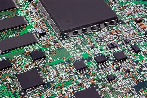
Modern PCB assembly processes leverage automation to achieve unprecedented levels of efficiency, precision, and scalability. By integrating advanced PCBA technologies, manufacturers can reduce manual intervention, minimize errors, and accelerate production cycles. For instance, automated pick-and-place systems and reflow soldering equipment ensure consistent component placement, while inline optical inspection (AOI) systems detect defects in real time.
A critical advantage of optimized PCB assembly lies in cost management. Strategic material sourcing, standardized design templates, and modular workflows help lower expenses without compromising quality. Consider the following comparison of traditional vs. automated approaches:
| Metric | Traditional Assembly | Automated PCBA |
|---|---|---|
| Production Speed | 8-12 hrs/batch | 2-4 hrs/batch |
| Error Rate | 5-8% | <1% |
| Labor Dependency | High | Minimal |
Scalability remains a cornerstone of streamlined workflows. Automated systems adapt seamlessly to high-volume orders, enabling manufacturers to meet fluctuating demand while maintaining tight tolerances. Additionally, data-driven analytics tools identify bottlenecks in PCB assembly lines, allowing for proactive adjustments to machine calibration or material flow.
To sustain competitiveness, manufacturers must prioritize continuous improvement in PCBA processes. This includes regular software updates for automation equipment, workforce training on emerging technologies, and adherence to industry standards like IPC-A-610. By aligning these elements, businesses can achieve shorter lead times, higher yield rates, and robust quality assurance across all production stages.
Automated PCB Assembly Boosts Production Speed
Modern PCB assembly processes leverage automation to dramatically accelerate production cycles while maintaining consistency. Advanced pick-and-place machines, for instance, can position components at speeds exceeding 25,000 placements per hour—far outpacing manual methods. These systems integrate with automated optical inspection (AOI) tools to instantly detect misalignments or soldering defects, reducing rework delays.
"Implementing PCBA automation isn’t just about speed; it’s about creating a repeatable workflow that minimizes human error," notes a manufacturing engineer at a leading electronics firm.
By optimizing machine programming and material handling, manufacturers achieve faster turnaround times without compromising precision. For example, closed-loop feedback systems adjust component placement in real time, ensuring alignment tolerances stay within ±0.05mm. Additionally, synchronized conveyor systems enable continuous processing, eliminating bottlenecks between soldering, inspection, and testing phases.
Transitioning to automated PCB assembly also supports scalability. Modular equipment configurations allow factories to adapt quickly to design changes or higher order volumes, making it easier to meet tight deadlines. This agility, paired with data-driven process monitoring, ensures that production speed improvements align with long-term quality goals—a critical balance for industries like aerospace and medical devices.
Cost-Effective PCB Board Assembly Strategies
Implementing cost-effective PCB assembly requires a balanced approach that integrates intelligent design, optimized workflows, and strategic material sourcing. A critical first step is leveraging design for manufacturability (DFM) principles to minimize rework and material waste. By collaborating with PCB assembly service providers during the design phase, engineers can identify potential bottlenecks, such as overly complex layouts or incompatible component footprints, which may escalate costs in later stages.
Adopting automated PCBA processes like pick-and-place systems and solder paste inspection (SPI) reduces labor expenses while ensuring consistent precision. For instance, combining surface-mount technology (SMT) with mixed-technology assembly allows manufacturers to handle both high-density components and through-hole parts efficiently. Bulk purchasing of common components, paired with just-in-time inventory management, further lowers material costs without compromising production timelines.
Another pivotal element is selecting standardized panel sizes to maximize board yield per substrate sheet, reducing raw material waste. Additionally, integrating in-line testing protocols during assembly—such as automated optical inspection (AOI)—helps catch defects early, minimizing costly post-production corrections. Partnering with suppliers offering volume discounts or consignment models for high-use components can also enhance cost efficiency.
Ultimately, achieving affordability in PCB assembly hinges on aligning design choices, process automation, and supply chain strategies to eliminate redundancies while maintaining rigorous quality standards. This holistic approach ensures that cost optimization does not come at the expense of reliability or performance.
Enhancing Quality in Automated Circuit Assembly
Modern PCB assembly processes rely on automated systems to achieve consistent precision, but maintaining quality demands more than just speed. Advanced PCBA lines integrate real-time inspection technologies, such as automated optical inspection (AOI) and X-ray testing, to detect microscopic defects like solder bridging or misaligned components. These systems analyze critical parameters — including solder paste volume and reflow oven temperature profiles — to ensure adherence to design specifications.
To minimize human error, manufacturers employ machine learning algorithms that adapt to component variations, optimizing placement accuracy for complex designs. For instance, high-speed pick-and-place machines equipped with vision systems can correct offsets in real time, reducing rework rates by up to 30%. Additionally, rigorous process validation protocols — such as first-article inspections and statistical process control (SPC) — create feedback loops that refine automation workflows.
While automation accelerates production, balancing speed with precision remains pivotal. Implementing closed-loop quality control in PCB assembly ensures defects are identified early, preventing costly downstream failures. By pairing intelligent automation with robust testing frameworks, manufacturers achieve both efficiency gains and reliability in PCBA outputs, aligning with industry standards like IPC-A-610.
Streamlined PCB Manufacturing Workflow Solutions
Modern PCB assembly processes demand precision and agility, driving manufacturers to adopt integrated workflow systems that eliminate bottlenecks. By synchronizing design, component sourcing, and PCBA production stages through digital twin technology, teams can simulate assembly outcomes before physical manufacturing begins. This proactive approach reduces material waste and identifies potential conflicts in component placement or soldering parameters.
Central to this optimization is the deployment of automated guided vehicles (AGVs) and smart conveyor systems, which ensure seamless material flow between surface-mount technology (SMT) lines and testing stations. Real-time monitoring via IoT-enabled sensors further enhances traceability, allowing engineers to track PCB assembly progress and address deviations instantly. For high-mix production environments, modular workflow designs enable rapid reconfiguration of assembly lines, cutting downtime during product changeovers by up to 40%.
Advanced PCBA workflows also integrate machine learning algorithms to predict maintenance needs for pick-and-place machines or reflow ovens, minimizing unplanned stoppages. Combined with standardized documentation protocols, these strategies create a cohesive manufacturing ecosystem where cycle time reductions and error-free outputs become repeatable achievements. Such systems not only accelerate time-to-market but also strengthen scalability for evolving production demands.
Smart Automation for Efficient PCB Assembly
The adoption of smart automation in PCB assembly processes has revolutionized manufacturing workflows by integrating robotic systems with AI-driven analytics. Modern PCBA lines now leverage automated pick-and-place machines, which achieve placement accuracies of ±0.025mm, significantly reducing human error. These systems utilize machine learning algorithms to optimize component placement sequences, cutting cycle times by up to 30% compared to manual methods.
A critical advantage lies in the seamless synchronization of IoT-enabled sensors with assembly equipment, enabling real-time monitoring of solder paste application and thermal profiles during reflow. This ensures consistent quality while minimizing rework rates. For instance, automated optical inspection (AOI) systems integrated into PCB assembly lines can detect defects as small as 10µm, ensuring compliance with stringent industry standards.
By leveraging smart automation, manufacturers achieve scalable production without compromising precision—a vital factor for high-mix, low-volume projects. Additionally, data collected from automated workflows supports predictive maintenance, further reducing downtime. This approach not only accelerates PCBA throughput but also aligns with broader goals of cost efficiency and waste reduction, as highlighted in earlier sections on workflow optimization. Transitioning to these technologies represents a strategic evolution for firms aiming to stay competitive in rapidly evolving electronics markets.
Reducing Lead Times in Circuit Board Production
Critical analysis of PCB assembly workflows reveals that minimizing production delays hinges on synchronizing design, component sourcing, and manufacturing stages. By adopting just-in-time inventory management for critical parts like ICs and connectors, manufacturers can eliminate bottlenecks caused by material shortages. Advanced PCBA lines equipped with high-speed pick-and-place systems and inline optical inspection (AOI) further compress cycle times by automating error detection and rework processes.
Transitioning to standardized design rules—such as unified pad geometries and panelization templates—reduces engineering back-and-forth, accelerating prototyping phases. Simultaneously, integrating real-time production monitoring tools enables rapid adjustments to machine utilization rates, preventing idle time in surface-mount technology (SMT) lines. For instance, embedding IoT sensors in reflow ovens and test jigs provides actionable data to preempt thermal profile deviations or fixture misalignments.
Moreover, leveraging cloud-based collaboration platforms ensures seamless communication between PCB assembly teams and OEM clients, trimming approval delays. When combined with predictive analytics for demand forecasting, these strategies create a closed-loop system that aligns material procurement with order volumes. The result? A PCBA ecosystem where lead times shrink by 30–40% without compromising the precision required for high-density interconnect (HDI) boards or mixed-technology assemblies.
PCB Assembly Process Optimization Techniques
Effective PCB assembly process optimization begins with analyzing workflow bottlenecks and implementing data-driven adjustments. By integrating PCBA-specific automation tools, manufacturers can minimize manual interventions, particularly in solder paste application and component placement stages. Advanced SMT (Surface Mount Technology) equipment paired with AI-powered optical inspection systems ensures consistent accuracy while reducing rework rates.
A critical strategy involves standardizing design-for-manufacturing (DFM) guidelines to prevent errors early in the circuit board assembly cycle. For instance, optimizing panelization layouts maximizes material utilization, lowering per-unit costs. Real-time monitoring of pick-and-place machines and reflow ovens through IoT-enabled sensors allows dynamic adjustments to temperature profiles and machine speeds, aligning output with quality benchmarks.
Additionally, adopting MES (Manufacturing Execution Systems) streamlines communication between PCB assembly stages, enabling just-in-time inventory management and faster defect resolution. Case studies show that combining predictive maintenance algorithms with lean manufacturing principles cuts downtime by up to 30% in PCBA lines. These refinements not only accelerate throughput but also enhance scalability, ensuring seamless adaptation to fluctuating order volumes without compromising precision.
Transitioning to such optimized workflows requires cross-departmental collaboration, particularly between design and production teams, to embed efficiency into every phase of circuit board assembly. This holistic approach lays the foundation for addressing subsequent challenges in maintaining precision during high-speed operations.
Maintaining Precision in High-Speed PCB Assembly
Achieving consistent accuracy in high-speed PCB assembly demands a meticulous balance between advanced technology and process control. As production velocities increase, even minor deviations in component placement or soldering can compromise PCBA reliability. Modern automated optical inspection (AOI) systems and laser-aligned pick-and-place machines are critical for ensuring micron-level precision, particularly when handling miniature components like 01005 packages or fine-pitch BGAs.
To sustain quality in PCB assembly, manufacturers deploy real-time thermal profiling during reflow soldering, which mitigates warping and ensures uniform solder joint formation. Additionally, high-speed assembly lines integrate closed-loop feedback mechanisms that automatically adjust parameters based on sensor data, reducing human error. For applications requiring signal integrity—such as 5G or aerospace systems—the use of impedance-controlled materials and rigorous testing protocols becomes non-negotiable.
Embedding design for manufacturability (DFM) principles early in the PCBA workflow further enhances precision. Collaboration between design engineers and assembly teams helps identify potential bottlenecks, such as inadequate pad spacing or incompatible component footprints, before prototyping. By combining these strategies, manufacturers can maintain sub-10μm placement tolerances while operating at cycle times under 30 seconds per board—proving that speed and precision in PCB assembly are not mutually exclusive.
Conclusion
As explored throughout this article, optimizing PCB assembly processes hinges on balancing speed, cost, and quality. By integrating automated solutions into PCBA workflows, manufacturers can achieve significant reductions in production lead times while maintaining exceptional precision. Advanced technologies like automated optical inspection (AOI) and surface-mount technology (SMT) not only accelerate throughput but also minimize human error, ensuring consistent output across high-volume orders.
To sustain competitiveness, adopting smart automation remains critical. Real-time monitoring systems and IoT-enabled machinery enable proactive adjustments, addressing potential bottlenecks before they escalate. Additionally, modular workflows in PCB assembly allow for scalable operations, adapting seamlessly to fluctuating demand without compromising efficiency.
Ultimately, the goal is to create a holistic manufacturing ecosystem where PCBA processes align with broader operational objectives. By prioritizing data-driven decision-making and investing in adaptive technologies, businesses can unlock long-term gains in productivity and cost-effectiveness. The future of PCB circuit board assembly lies in continuous refinement—leveraging innovation to stay ahead in an ever-evolving industry.
Frequently Asked Questions
What are the primary benefits of automating PCB assembly processes?
Automation in PCBA reduces manual intervention, minimizes human error, and accelerates production cycles. Advanced pick-and-place systems and reflow ovens ensure consistent solder joint quality, while automated optical inspection (AOI) enhances defect detection accuracy.
How can manufacturers balance cost reduction with quality in PCB assembly?
Adopting design for manufacturability (DFM) principles optimizes component placement and material usage, lowering waste. Pairing this with standardized surface-mount technology (SMT) workflows ensures repeatability, reducing rework costs without compromising reliability.
What challenges arise in high-volume PCB circuit board assembly?
Scaling production often exposes bottlenecks in component sourcing or testing phases. Implementing smart inventory management and integrating real-time monitoring systems help mitigate delays, ensuring seamless alignment between supply chain and assembly lines.
How does automated PCBA impact lead times?
By streamlining solder paste application, component placement, and testing, automation cuts lead times by up to 40%. Parallel processing in multi-stage assembly lines further eliminates downtime between production phases.
Can small-batch PCB assembly benefit from automation?
Yes. Modular automation tools, such as programmable stencil printers and compact AOI systems, allow flexible scaling. This enables cost-effective low-volume PCBA without sacrificing precision or turnaround speed.
Ready to Optimize Your PCB Assembly Process?
Explore advanced solutions tailored for your manufacturing needs. Click here to discover how Andwin PCB can elevate your PCB assembly efficiency and reduce operational costs today.