Streamlining PCB Manufacturing and Assembly for Peak Efficiency
Key Takeaways
Effective PCB manufacturing and assembly hinges on harmonizing design, prototyping, and production phases. Start by optimizing design for manufacturability (DFM) to minimize rework during PCBA. Tools like automated design checks reduce errors early, accelerating timelines. For prototyping, prioritize rapid-turn fabrication paired with automated optical inspection (AOI) to validate designs before scaling.
| Traditional Approach | Modern Strategy |
|---|---|
| Manual design reviews | DFM-integrated CAD tools |
| Prototype iterations | 3D-printed PCB mockups |
| Post-assembly testing | In-line AOI systems |
Tip: "Align your design team with fabrication partners during prototyping to eliminate mismatches in material specifications or layer alignment."
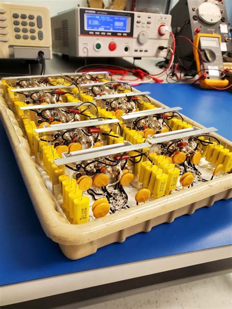
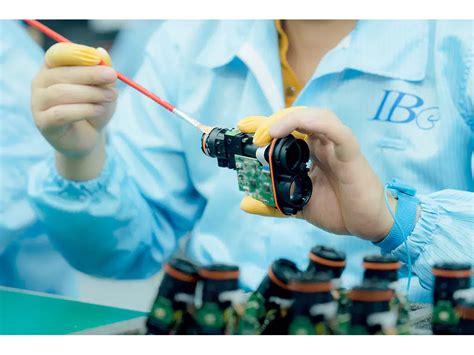
Leverage automation in PCB assembly—such as pick-and-place machines and reflow ovens—to ensure precision in high-volume production. Integrate smart quality control systems, like AI-driven defect detection, to maintain consistency. For cost efficiency, standardize components and adopt panelization to maximize substrate utilization. Testing phases should include thermal cycling and functional validation to guarantee reliability.
To streamline workflows, adopt unified platforms that synchronize PCB assembly data across design, procurement, and logistics teams. For deeper insights into fabrication standards, review this guide on fabrication and assembly drawings. By merging these strategies, manufacturers achieve faster turnarounds without compromising on PCBA quality.
Optimize PCB Design Processes
Effective PCB assembly begins with optimizing design workflows to eliminate production bottlenecks. Early-stage design choices directly impact PCBA outcomes, making it critical to adopt design-for-manufacturability (DFM) principles. By collaborating with fabrication partners during schematic development, engineers can identify potential issues like improper trace spacing or component placement, reducing rework during PCB assembly. Advanced ECAD tools now integrate real-time DFM checks, flagging violations such as insufficient solder mask clearance or mismatched pad sizes.
Leveraging modular design frameworks further accelerates development. Reusing validated circuit blocks—such as power supply modules or signal conditioning circuits—minimizes design iterations while ensuring compatibility with automated PCBA lines. Thermal management and signal integrity simulations should precede layout finalization, as overheating or EMI risks discovered post-production lead to costly delays. For high-density designs, embedded component technology (ECT) reduces layer counts, trimming material costs and assembly time.
Finally, aligning component libraries with manufacturer inventories prevents procurement delays. Designers should prioritize industry-standard packages (e.g., 0402 resistors, QFN ICs) over niche footprints to ensure seamless integration into PCB assembly workflows. Cross-referencing part availability in platforms like Octopart or SiliconExpert during BOM creation avoids last-minute substitutions. By implementing these strategies, teams ensure designs transition smoothly from prototyping to volume PCBA, maintaining alignment with cost and timeline targets.
Quick PCB Prototyping Methods
Rapid prototyping is critical for accelerating PCB assembly timelines while maintaining design integrity. Modern approaches leverage design-for-manufacturing (DFM) software to preemptively flag layout issues, reducing iterative revisions. Advanced PCBA suppliers now combine additive manufacturing techniques, such as 3D-printed circuit layers, with laser-direct structuring to produce functional prototypes within 48 hours. These methods enable engineers to validate signal integrity and thermal performance before committing to full-scale production.
Automated optical inspection (AOI) systems further streamline prototyping by instantly identifying soldering defects or component misalignments, ensuring compliance with IPC-A-610 standards. For high-mix projects, modular fixture designs allow swift reconfiguration between prototype batches, cutting downtime by up to 70%. By integrating PCB assembly data with cloud-based analytics teams can predict material bottlenecks and optimize solder paste application parameters in real time.
Adopting iterative testing protocols during prototyping—such as boundary-scan diagnostics—helps isolate faults at the board level, preventing cascading failures in later PCBA stages. This proactive alignment between prototyping and mass production workflows ensures seamless scalability, making it possible to transition from concept to market-ready products in record time.
Automation in PCB Assembly
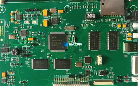
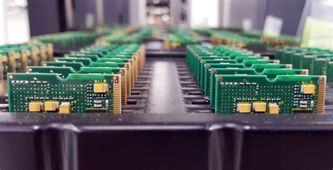
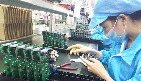
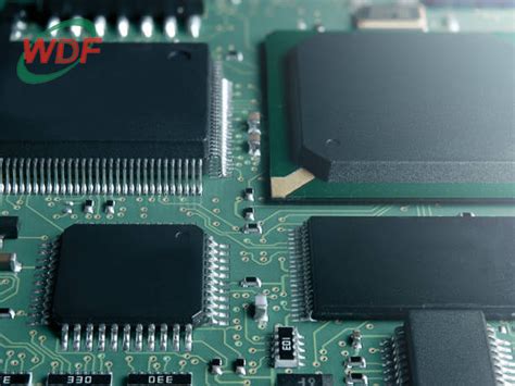
Modern PCB assembly workflows increasingly rely on automated systems to achieve precision and scalability in high-volume production. By integrating robotic placement machines, automated optical inspection (AOI), and AI-driven process control, manufacturers minimize human error while accelerating PCBA cycles. For instance, surface-mount technology (SMT) lines now utilize advanced pick-and-place robots capable of positioning components at speeds exceeding 50,000 placements per hour, ensuring consistent accuracy even for micro-sized parts.
A critical advantage of automation lies in its seamless compatibility with design-for-manufacturing (DFM) principles. Software-driven systems analyze CAD files to optimize component placement, reducing material waste and rework. This synergy between digital design and physical assembly is further enhanced by real-time monitoring tools, which track metrics like solder paste viscosity and thermal profiles during reflow processes.
To maintain reliability in sensitive environments, some facilities adopt Class 10000 cleanrooms for PCBA stages involving fine-pitch ICs or medical-grade electronics. Automated conveyor systems within these controlled environments ensure uninterrupted workflows while mitigating contamination risks.
Transitioning to automated PCB assembly not only boosts throughput but also strengthens traceability. Machine-learning algorithms analyze historical production data to predict potential defects, enabling proactive adjustments. As a result, manufacturers achieve tighter tolerances in impedance control and signal integrity—key factors for next-generation IoT and automotive applications.
Smart Quality Control Systems
Modern PCB assembly workflows demand precision at every stage, making intelligent quality control indispensable. By integrating PCBA-specific inspection technologies like automated optical inspection (AOI) and X-ray imaging, manufacturers can detect microscopic defects—from solder bridging to misaligned components—with sub-micron accuracy. These systems employ machine learning algorithms to analyze historical production data, refining defect recognition patterns over time and reducing false positives by up to 40%.
For high-volume PCB assembly lines, real-time process adjustments are critical. Advanced systems monitor variables such as solder paste viscosity and reflow oven temperatures, automatically correcting deviations before they impact yield. This proactive approach minimizes rework cycles, ensuring PCBA outputs meet IPC-A-610 standards without delaying timelines.
Predictive analytics further elevate quality assurance by identifying potential failure modes in design files or component batches early in production. Coupled with traceability software, every PCBA unit is logged with granular data—from component lot numbers to test results—streamlining compliance audits and post-production troubleshooting.
By aligning PCB assembly quality protocols with Industry 4.0 principles, manufacturers achieve tighter process control while maintaining scalability—a cornerstone for electronics workflows prioritizing both reliability and efficiency.
Cost-Effective Manufacturing Tips
Achieving cost efficiency in PCB assembly requires strategic planning across design, material selection, and production workflows. Start by optimizing designs for manufacturability (DFM) to minimize waste and reduce rework. For instance, simplifying component placement and adhering to standardized panel sizes can lower material costs. Leveraging design software with built-in DFM checks ensures compatibility with automated PCBA processes, avoiding delays caused by manual corrections.
Collaborating with suppliers to negotiate bulk pricing for high-quality substrates and components is another proven tactic. Consider hybrid approaches, such as combining standard and custom parts, to balance performance and affordability. Implementing automation in PCB assembly—like pick-and-place machines and reflow soldering systems—not only accelerates throughput but also enhances consistency, reducing defects that inflate costs. For deeper insights into automation trends, explore this analysis.
Additionally, adopting predictive maintenance for equipment minimizes downtime, while smart inventory management prevents overstocking. Integrating real-time monitoring tools into PCBA lines further identifies inefficiencies, enabling data-driven adjustments. By aligning design, procurement, and production phases, manufacturers can achieve scalable cost savings without compromising quality—a critical advantage in competitive electronics markets.
Testing Ensures PCB Reliability
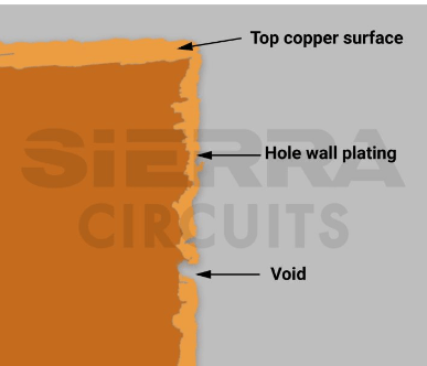
Rigorous testing protocols form the backbone of dependable PCB assembly, ensuring that every PCBA meets stringent performance standards. Advanced verification methods, such as In-Circuit Test (ICT) and Automated Optical Inspection (AOI), systematically identify defects in solder joints, component alignment, and electrical connectivity. These processes are critical for catching early-stage flaws that could compromise functionality in high-stakes applications, from medical devices to aerospace systems.
Beyond basic inspections, environmental stress testing—including thermal cycling and vibration simulations—validates a board’s resilience under real-world operating conditions. For instance, Gold Phoenix PCB employs accelerated life testing to predict long-term reliability, reducing field failure risks by over 30%. Modern PCBA workflows also integrate Design for Testing (DFT) principles, embedding test points during layout to streamline diagnostics. This proactive approach minimizes rework cycles while aligning with ISO 9001 and IPC-A-610 compliance requirements.
By coupling automated test equipment with data analytics, manufacturers achieve traceable quality metrics, enabling continuous improvement in PCB assembly processes. This comprehensive approach not only safeguards product integrity but also reinforces stakeholder confidence in mission-critical electronics.
Streamlined Workflow Strategies
Achieving peak efficiency in PCB assembly requires harmonizing design, prototyping, and production into a unified workflow. By adopting integrated design platforms, engineers can identify manufacturability issues early, reducing costly revisions during PCBA stages. For instance, synchronizing CAD software with assembly-line simulations allows teams to visualize component placements and thermal dynamics before physical prototyping begins.
Transitioning to automated documentation systems further minimizes delays. Tools like AtechPCB’s collaborative platform enable real-time updates between design and manufacturing teams, ensuring specifications remain aligned. Additionally, lean principles—such as batch size optimization and just-in-time material sourcing—trim excess inventory while maintaining production agility.
Automation extends beyond machinery; workflow orchestration software tracks progress across PCB assembly stages, flagging bottlenecks in solder paste application or component mounting. Pairing this with predictive analytics helps preempt equipment maintenance needs, sustaining uptime during high-volume PCBA runs. Such strategies not only accelerate timelines but also enhance reproducibility, critical for scaling operations without compromising precision.
Conclusion
The journey toward optimized PCB manufacturing and assembly hinges on harmonizing design, production, and quality assurance into a cohesive workflow. By aligning PCB design practices with automation in PCBA, manufacturers achieve precision at scale while minimizing human error. Advanced smart quality control systems further ensure that defects are identified early, reducing rework costs and accelerating time-to-market.
Adopting iterative prototyping and rigorous testing protocols not only validates reliability but also creates a feedback loop for continuous improvement. For businesses prioritizing efficiency, integrating cost-effective manufacturing strategies—such as modular tooling and material optimization—can unlock significant savings without compromising performance.
Ultimately, the success of PCB assembly projects relies on balancing speed with meticulous attention to detail. Leveraging PCBA innovations like AI-driven inspection and real-time monitoring transforms traditional workflows into agile, future-ready operations. By embedding these principles into every stage—from concept to final product—organizations can sustainably meet evolving demands while maintaining competitive margins.
FAQs
What is the difference between PCB assembly and PCBA?
PCB assembly refers to the process of attaching electronic components to a bare circuit board, while PCBA (Printed Circuit Board Assembly) denotes the completed board with all components mounted and ready for integration. Both terms are often used interchangeably, but PCBA emphasizes the end product’s functional state.
How does automation improve PCB assembly quality?
Automation technologies like surface-mount technology (SMT) and automated optical inspection (AOI) ensure consistent placement accuracy and defect detection. This reduces human error, accelerates high-volume production, and maintains compliance with industry standards such as IPC-A-610.
What quality control measures are critical in PCBA?
In-circuit testing (ICT) and functional testing validate electrical performance and operational reliability. Implementing statistical process control (SPC) tools further monitors production variations, ensuring defects are identified early in the PCB assembly workflow.
Can PCB assembly be cost-effective for small batches?
Yes. Partnering with manufacturers offering flexible prototyping services minimizes upfront costs. Modular designs and panelization strategies also optimize material usage, making low-volume PCBA projects economically viable.
Why is testing integral to PCB reliability?
Rigorous testing simulates real-world conditions—thermal cycling, vibration, and humidity tests—to uncover weaknesses. This prevents field failures and extends the lifespan of PCBA units, particularly in aerospace or medical applications.
How do streamlined workflows benefit PCB manufacturing?
Integrated design-for-manufacturability (DFM) checks and digital twin simulations reduce rework cycles. This alignment between design and PCB assembly stages cuts lead times by up to 30%, enhancing time-to-market efficiency.
Transform Your Production Line Today
Ready to elevate your PCB assembly capabilities? Click here to explore advanced solutions tailored for precision and scalability.