Streamlining Prototype PCB Assembly with Expert Manufacturers

Key Takeaways
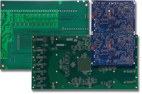
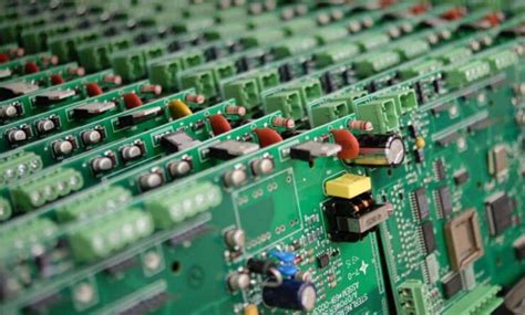
When partnering with PCB assembly experts, businesses gain access to precision engineering that minimizes design flaws early in the prototyping phase. Specialized PCBA providers leverage advanced technologies like automated optical inspection (AOI) and 3D solder paste dispensing to ensure rapid PCB prototype turnaround, often delivering functional boards within 48–72 hours.
A critical advantage lies in balancing cost-efficiency with quality. Reputable manufacturers optimize material selection and assembly workflows, reducing expenses without compromising reliability. For instance:
| Factor | Expert Manufacturer | Traditional Methods |
|---|---|---|
| Turnaround Time | 2–5 days | 7–14 days |
| Defect Rate | <0.5% | 2–3% |
| Scalability | Seamless transition to volume | Limited batch flexibility |
Additionally, PCB prototype quality assurance is reinforced through multi-stage testing protocols, including in-circuit testing (ICT) and functional validation. This ensures prototypes meet exact specifications before moving to mass production. By integrating advanced PCB prototyping tech such as impedance-controlled routing and HDI layouts, manufacturers enable designers to fast-track innovation while mitigating risks.
Collaboration with PCBA specialists also simplifies compliance with industry standards like IPC-A-610, ensuring prototypes align with regulatory requirements from the outset. This alignment streamlines development cycles, allowing teams to focus on iterative testing and design refinement.
Precision PCB Prototyping
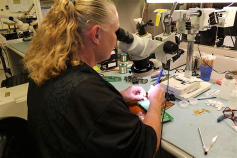
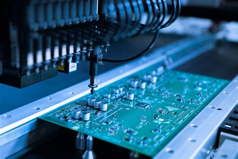
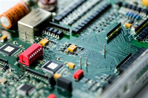
Modern electronics development hinges on precision PCB prototyping to validate designs before full-scale production. Specialized PCB assembly manufacturers leverage advanced techniques to ensure components are placed with micron-level accuracy, critical for high-density boards and complex circuits. Precision-driven workflows integrate laser-cut stencils, automated pick-and-place systems, and reflow soldering to achieve consistent results across prototype batches.
Tip: When selecting a PCBA partner, verify their capability to handle fine-pitch components (≤0.4mm) and ultra-thin substrates, as these directly impact prototyping accuracy.
Key factors in precision prototyping include material selection (e.g., high-Tg laminates for thermal stability) and adherence to IPC-A-610 standards for solder joint quality. Advanced manufacturers employ 3D AOI (Automated Optical Inspection) systems to detect defects like micro-shorts or misaligned ICs, reducing iterative delays. By combining rigid-flex PCB expertise with real-time design feedback, engineers can refine layouts for manufacturability without compromising performance.
Transitioning from prototype to mass production requires seamless data handoff between design teams and PCB assembly specialists. This alignment ensures that tolerances, layer stackups, and testing protocols remain consistent, accelerating time-to-market while mitigating risks in later stages.
Rapid PCB Prototype Turnaround
In today’s competitive electronics landscape, accelerating PCB assembly timelines is critical for maintaining innovation momentum. Expert PCBA manufacturers leverage advanced machinery and streamlined workflows to deliver prototype boards in as little as 24–48 hours, ensuring design validation cycles stay agile. By integrating automated pick-and-place systems and precision soldering technologies, these specialists minimize manual errors while optimizing production speed.
A key driver of rapid turnaround is the adoption of just-in-time inventory management, which reduces delays in component sourcing. Partnering with trusted suppliers allows manufacturers to secure high-quality parts swiftly, even for complex designs. Additionally, digital collaboration tools enable real-time feedback loops between engineers and production teams, resolving potential bottlenecks before they impact timelines.
For startups and enterprises alike, fast PCB prototype delivery translates to quicker testing iterations and faster market entry. However, speed must not compromise reliability. Reputable PCBA providers balance urgency with rigorous quality checks, employing automated optical inspection (AOI) and functional testing to ensure prototypes meet performance benchmarks. This dual focus on velocity and precision positions businesses to refine designs efficiently while mitigating risks in later production stages.
Affordable PCB Assembly Services
Balancing cost efficiency with technical precision is critical in PCB assembly, particularly for prototyping phases where budget constraints often intersect with quality demands. Leading prototype PCB assembly manufacturers leverage economies of scale and advanced PCBA workflows to deliver cost-optimized solutions without compromising performance. By integrating automated assembly processes and strategic component sourcing, these providers reduce material waste and labor costs, passing savings to clients.
For startups and SMEs, volume-tiered pricing models enable access to high-quality PCB assembly services even for low-volume orders. Additionally, streamlined logistics and partnerships with global suppliers ensure timely procurement of components, further lowering expenses. Advanced PCBA techniques, such as surface-mount technology (SMT) and precision soldering, minimize rework risks, aligning affordability with reliability.
To enhance affordability, manufacturers often offer design-for-manufacturability (DFM) checks, identifying potential cost drivers early in the prototyping cycle. This proactive approach prevents costly redesigns and accelerates time-to-market. Whether for iterative testing or pre-production validation, partnering with specialists in PCB assembly ensures prototypes meet both technical specifications and budgetary targets, laying a foundation for scalable innovation.
PCB Prototype Quality Assurance
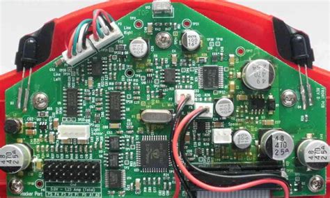
Ensuring reliability in PCB assembly begins with rigorous quality assurance protocols tailored for prototyping phases. Expert manufacturers implement automated optical inspection (AOI) and X-ray inspection to detect microscopic flaws in solder joints, component alignment, and layer alignment. These processes are critical for PCBA prototypes, where even minor defects can derail testing outcomes or lead to costly redesigns. Advanced manufacturers adhere to IPC-A-610 and IPC-J-STD-001 standards, guaranteeing that assemblies meet functional and durability benchmarks before moving to mass production.
To maintain consistency, trusted providers integrate real-time monitoring across soldering temperatures, paste application, and placement accuracy. This minimizes variability, especially in high-density designs with fine-pitch components. Additionally, functional testing simulates real-world operating conditions to validate signal integrity, power distribution, and thermal performance. By combining these strategies with traceability systems, manufacturers ensure defects are logged and addressed at the source, reducing iteration cycles.
For startups and enterprises alike, partnering with PCB assembly specialists who prioritize quality assurance translates to prototypes that accurately reflect design intent. This alignment between PCBA precision and testing rigor not only accelerates development timelines but also strengthens confidence in transitioning from prototyping to full-scale manufacturing.
Streamline Development with Experts
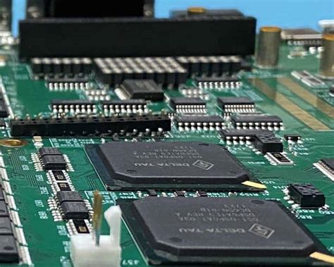
Collaborating with specialized PCB assembly manufacturers enables teams to focus on core design innovation while experts handle technical execution. These partners bring deep industry knowledge to optimize layouts for manufacturability, select appropriate components, and implement PCBA processes that align with project requirements. By leveraging their expertise in high-density interconnect (HDI) configurations and surface-mount technology, developers avoid common prototyping pitfalls that delay timelines.
Seasoned manufacturers employ design-for-manufacturing (DFM) analysis tools to identify potential issues early, ensuring prototypes meet both functional and compliance standards. Their structured workflow integrates PCB assembly with rigorous functional testing, creating a closed-loop system that validates designs before full-scale production. For startups and enterprises alike, this partnership model reduces iterative redesign cycles by 30-45%, accelerating product validation phases.
Moreover, expert providers maintain component libraries and supplier networks to source rare or obsolete parts, resolving material bottlenecks. Their ability to balance PCBA precision with scalable solutions ensures prototypes transition smoothly to mass production. This collaborative approach transforms complex development challenges into predictable, milestone-driven processes—a critical advantage in competitive tech markets.

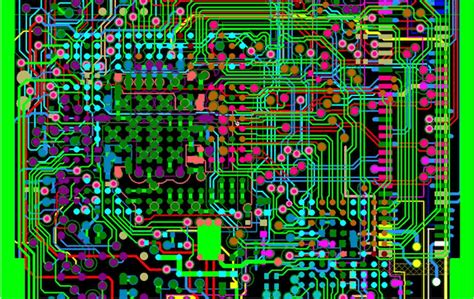
Advanced PCB Prototyping Tech
Modern PCB assembly processes leverage cutting-edge technologies to address the complexities of prototyping. Innovations such as high-density interconnect (HDI) substrates and flexible printed circuits enable manufacturers to accommodate intricate designs while maintaining reliability. Advanced PCBA workflows now integrate automated optical inspection (AOI) systems and AI-driven defect detection, ensuring precision at micron-level tolerances. These tools minimize human error and accelerate validation cycles, critical for iterative prototyping.
The adoption of 3D printing for rapid tooling and laser direct imaging (LDI) for ultra-fine trace patterning further enhances design flexibility. Such technologies allow expert manufacturers to support mixed-material boards, RF components, and embedded systems—key requirements for IoT and wearable devices. By combining PCB assembly expertise with real-time data analytics, teams can predict thermal performance and signal integrity issues early, reducing costly redesigns.
Transitioning from concept to functional prototype demands seamless collaboration between design engineers and PCBA specialists. Cloud-based platforms enable instant feedback on manufacturability, while modular assembly lines ensure scalability from low-volume batches to pre-production runs. This synergy between advanced tech and engineering acumen shortens development timelines, aligning with the broader goal of accelerating innovation in electronics prototyping.
Fast-Track PCB Prototype Innovation
In today’s competitive electronics landscape, accelerating innovation requires collaboration with PCB assembly experts who specialize in rapid prototyping. Leading prototype PCB assembly manufacturers leverage advanced fabrication techniques and automated PCBA processes to reduce development cycles from weeks to days. By combining high-speed pick-and-place systems with precision soldering technologies, these partners ensure first-run success for complex designs, minimizing costly revisions.
Critical to this acceleration is the integration of real-time design feedback during PCB assembly, enabling engineers to validate functionality early. For instance, PCBA providers often employ in-house prototyping labs equipped with 3D AOI (Automated Optical Inspection) and X-ray testing, ensuring electrical integrity before full-scale production. This proactive approach not only streamlines iterations but also aligns with agile development methodologies, allowing teams to test multiple configurations swiftly.
Moreover, partnerships with specialized prototype PCB assembly manufacturers provide access to flexible material sourcing and hybrid manufacturing models, balancing speed with cost efficiency. Whether refining IoT devices or high-frequency circuits, the ability to iterate rapidly without compromising quality transforms conceptual designs into market-ready solutions. By prioritizing PCB assembly precision and PCBA scalability, innovators gain a critical edge in bringing cutting-edge technologies to life faster than ever.
Seamless Prototyping Solutions
Achieving seamless prototyping requires a harmonized workflow between design teams and PCB assembly experts. Leading prototype PCB assembly manufacturers leverage advanced PCBA processes to bridge the gap between conceptual designs and functional prototypes, ensuring minimal friction during iterative development. By integrating automated solder paste application, precision component placement, and real-time quality monitoring, these specialists eliminate bottlenecks that traditionally delay prototyping phases.
A critical advantage lies in their ability to support rapid iteration—whether adjusting trace widths, swapping components, or validating firmware compatibility. Advanced PCB assembly platforms enable manufacturers to execute design changes within hours, reducing downtime between testing cycles. Additionally, transparent communication channels ensure engineers receive immediate feedback on manufacturability and cost drivers, allowing for informed adjustments before finalizing designs.
For startups and established firms alike, partnering with PCBA professionals translates to risk mitigation during prototyping. Rigorous pre-production checks, including thermal stress tests and signal integrity analysis, identify potential flaws early, preventing costly revisions later. This collaborative approach not only accelerates time-to-market but also ensures prototypes meet performance benchmarks, paving the way for smooth transitions to mass production.
Conclusion
In today’s fast-paced electronics landscape, partnering with specialized PCB assembly providers ensures prototypes evolve from concept to reality with unmatched efficiency. Expert manufacturers leverage advanced manufacturing technologies and rigorous testing protocols to deliver PCBA solutions that align with stringent quality benchmarks while accelerating time-to-market. By integrating rapid prototyping workflows with scalable PCB assembly processes, these partners mitigate risks in design validation and functional testing, ensuring seamless transitions to full-scale production.
The synergy between precision engineering and agile project management enables manufacturers to address complex technical requirements without compromising cost-effectiveness. Whether refining high-frequency circuits or optimizing thermal management, a trusted PCBA partner provides the technical foundation to iterate designs confidently. This collaborative approach not only streamlines development cycles but also empowers innovators to focus on core competencies, knowing their prototypes are built on reliable, industry-tested frameworks. Ultimately, the right manufacturing alliance transforms prototyping from a logistical challenge into a strategic advantage.
FAQs
What distinguishes prototype PCB assembly from standard production runs?
Prototype PCBA focuses on low-volume, high-precision builds to validate designs before mass production. Manufacturers employ specialized tools and rigorous testing protocols to ensure functionality, whereas standard runs prioritize scalability over iterative adjustments.
How do expert manufacturers ensure rapid turnaround for prototype PCB assembly?
Leading providers utilize automated PCB assembly workflows, component sourcing networks, and concurrent engineering practices. By integrating design feedback loops and real-time quality checks, they compress timelines without compromising reliability.
Are cost-effective solutions viable for complex prototype PCBA projects?
Yes. Advanced manufacturers optimize material selection, panelization strategies, and testing phases to reduce waste. Modular PCB assembly approaches allow iterative refinements, preventing costly redesigns in later stages.
What quality assurance measures apply to prototype PCB assembly?
Reputable firms implement IPC-A-610 compliance, automated optical inspection (AOI), and functional testing. These steps verify solder integrity, component alignment, and electrical performance, ensuring prototypes meet production-grade standards.
Why collaborate with specialized PCB assembly partners for prototyping?
Experts provide design-for-manufacturability (DFM) insights, component lifecycle management, and risk mitigation strategies. Their expertise accelerates development cycles while aligning prototypes with long-term production goals.
Accelerate Your Project with Professional PCB Assembly Services – Click Here to Start
Can prototype PCBA services support mixed-technology boards?
Absolutely. Advanced manufacturers handle hybrid designs combining surface-mount (SMT), through-hole (THT), and embedded components. Flexible PCB assembly capabilities ensure compatibility with diverse prototyping requirements.