Streamlining Quick PCB Assembly for Faster Product Deployment

Key Takeaways
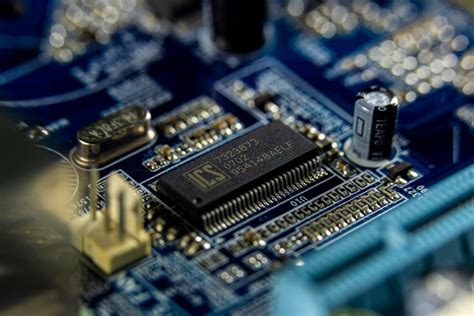
Effective PCB assembly relies on balancing speed, precision, and scalability. Implementing automated optical inspection (AOI) systems minimizes human error while accelerating prototyping cycles, ensuring consistent quality even in high-volume PCBA runs. Modular design practices, such as standardized component libraries, reduce rework and enable faster iterations.
Tip: Prioritize component sourcing partnerships early in the design phase to avoid supply chain bottlenecks during rapid PCB assembly.
Advanced pick-and-place robotics paired with intelligent solder paste dispensers can cut assembly time by up to 40%, particularly for complex multilayer boards. Meanwhile, integrating real-time analytics into PCBA workflows helps identify process inefficiencies—like solder joint defects or misalignments—before they escalate.
For teams targeting compressed timelines, adopting design-for-manufacturability (DFM) principles ensures compatibility with automated PCB assembly lines. This approach not only reduces post-production adjustments but also supports seamless scaling from prototypes to mass production.
"Speed without precision is counterproductive in PCBA," notes a leading hardware engineer. "Optimizing thermal management and signal integrity during rapid builds prevents costly redesigns post-prototyping."
By synchronizing these strategies, manufacturers achieve faster time-to-market without compromising the reliability of PCB assembly outcomes.

Automated PCB Assembly Speed Strategies
Modern PCB assembly processes demand strategic integration of automation to achieve faster turnaround without compromising quality. By implementing automated optical inspection (AOI) systems and high-speed pick-and-place machines, manufacturers can reduce manual intervention while ensuring PCBA accuracy. For instance, robotic soldering arms programmed with machine learning algorithms adapt to component variations, slashing assembly errors by up to 40% compared to traditional methods.
A critical speed-enhancing tactic involves synchronizing design files with automated assembly lines. Designers using EDA tools (Electronic Design Automation) can pre-validate layouts for manufacturability, minimizing rework delays. Below is a comparison of key automation strategies:
| Strategy | Impact Area | Time Reduction |
|---|---|---|
| Robotic Component Placement | Assembly Accuracy | 25-35% |
| Real-Time AOI Feedback | Defect Detection | 50-60% |
| Smart Inventory Management | Material Procurement | 20-30% |
To further accelerate PCB assembly, factories are adopting closed-loop workflows where data from testing phases directly informs upstream processes. This approach reduces iterative prototyping cycles, enabling faster transitions from PCBA validation to mass production. However, balancing speed with thermal management and signal integrity remains non-negotiable, necessitating advanced simulation tools integrated into automated systems.
By prioritizing modular automation frameworks, manufacturers ensure scalability across varying batch sizes—critical for industries requiring both rapid prototyping and high-volume PCB assembly.

Optimizing Rapid Prototyping Workflows
Efficient PCB assembly begins with refining prototyping workflows to eliminate bottlenecks. By implementing design-for-manufacturability (DFM) checks early in the design phase, engineers can preemptively address issues that delay PCBA timelines. Automated optical inspection (AOI) systems further streamline validation, ensuring component placement accuracy while reducing manual rework.
Advanced software tools, such as real-time collaboration platforms, synchronize cross-functional teams, enabling faster iteration cycles. For instance, integrating simulation-driven prototyping allows teams to test thermal performance or signal integrity virtually before physical PCB assembly begins. This reduces costly mid-process revisions and accelerates feedback loops.
Modular tooling and standardized component libraries also play a critical role. By leveraging pre-validated footprints and solder profiles, manufacturers minimize setup times for PCBA batches. Additionally, adopting hybrid manufacturing models—combining rapid-turn services for prototypes with scalable production lines—ensures seamless transitions from testing to full-scale deployment.
To maintain momentum, prioritize data-driven decision-making. Analytics from past projects can identify recurring delays, enabling proactive adjustments to workflow parameters. Pairing this with agile supplier networks ensures just-in-time material availability, further compressing lead times without compromising quality.
Precision Techniques for Quick PCB Builds
Achieving rapid PCB assembly without compromising quality demands meticulous attention to precision engineering. Modern automated optical inspection (AOI) systems play a pivotal role in verifying solder joint integrity and component placement accuracy during PCBA, ensuring defects are caught in real time. Advanced pick-and-place machines equipped with vision-guided alignment further enhance precision, enabling micron-level positioning of components even in high-speed production environments.
Material selection also contributes significantly to reliable quick builds. Using low-temperature co-fired ceramics (LTCC) or high-frequency laminates minimizes signal loss in complex designs, while laser-direct imaging (LDI) streamlines photolithography for finer trace resolutions. For prototyping, design-for-manufacturability (DFM) software identifies potential bottlenecks early, allowing engineers to adjust layouts for optimal PCB assembly efficiency.
A critical yet often overlooked aspect is thermal management. Implementing controlled impedance routing and thermal relief pads prevents warping during reflow soldering, maintaining structural integrity across rapid thermal cycles. By integrating these precision techniques, manufacturers can scale PCBA workflows without sacrificing repeatability—key to delivering consistent results in fast-paced development cycles.
Accelerating Time-to-Market With PCB Tech
Modern advancements in PCB assembly (PCBA) technologies are redefining how quickly products transition from concept to market-ready solutions. By integrating automated pick-and-place systems and AI-driven inspection tools, manufacturers can drastically reduce manual intervention, minimizing errors and shortening production timelines. For instance, surface-mount technology (SMT) enables high-speed placement of components, while real-time analytics optimize material usage and workflow efficiency. These innovations are critical for industries requiring rapid iterations, such as IoT devices and consumer electronics, where delays in PCB assembly can derail entire product launches.
To further accelerate time-to-market, companies are adopting modular design frameworks that standardize component layouts across projects. This approach not only streamlines PCBA processes but also ensures compatibility with scalable manufacturing systems. Additionally, leveraging cloud-based collaboration platforms allows cross-functional teams to synchronize design changes instantly, preventing bottlenecks in prototyping phases. By prioritizing PCB assembly precision alongside speed, businesses achieve a balance between agility and reliability—key to maintaining competitive advantage in fast-paced markets.
Transitioning seamlessly from prototyping to mass production requires strategic alignment between design engineers and manufacturing partners, ensuring that every iteration adheres to both technical specifications and market deadlines.
Scalable Solutions for Fast PCB Production
Achieving scalability in PCB assembly requires a strategic balance between automation, flexible manufacturing systems, and adaptive supply chain management. Modern high-mix, low-volume production demands solutions that can seamlessly transition from prototyping to full-scale manufacturing without compromising speed. By integrating PCBA workflows with modular manufacturing platforms, companies can dynamically allocate resources based on project complexity or order volume. For instance, cloud-based process control systems enable real-time adjustments to soldering profiles or component placement algorithms, ensuring consistent quality across varying batch sizes.
Advanced PCB assembly lines now incorporate hybrid automation, combining robotic pick-and-place machines with AI-driven optical inspection tools. This approach minimizes manual intervention while maintaining precision—critical for applications like IoT devices or wearable electronics. Additionally, scalable PCBA solutions leverage standardized design libraries and pre-validated component footprints, reducing engineering overhead during design-for-manufacturing (DFM) stages. Partnering with suppliers offering just-in-time inventory models further accelerates turnaround, as critical components are staged for rapid deployment. By aligning these strategies, businesses can efficiently scale production capacities to meet fluctuating market demands, ensuring faster product launches without overextending operational resources.
Streamlined PCB Assembly Best Practices
Implementing streamlined PCB assembly processes requires a strategic balance between speed and precision. Central to this approach is the adoption of standardized design templates that minimize revisions during PCBA (printed circuit board assembly). By integrating automated optical inspection (AOI) systems, manufacturers can rapidly identify defects without compromising throughput, ensuring consistent quality even in high-speed production environments.
A critical best practice involves optimizing component sourcing to align with lead times, reducing bottlenecks in quick PCB assembly workflows. Leveraging surface-mount technology (SMT) for high-density layouts further accelerates placement accuracy, while modular assembly lines enable seamless scaling between prototyping and full-scale production. Additionally, employing design for manufacturing (DFM) principles early in the development cycle prevents costly rework, aligning PCB assembly timelines with aggressive product launch schedules.
To maintain agility, many teams now utilize real-time data analytics to monitor assembly metrics, enabling rapid adjustments to material flows or machine calibration. This proactive approach not only sustains the pace of PCBA but also fortifies scalability—a cornerstone for industries requiring both speed and repeatability in electronics manufacturing.
Reducing Delays in PCB Prototyping Cycles
Minimizing bottlenecks in PCB assembly requires addressing both technical and logistical challenges. One critical approach involves integrating automated optical inspection (AOI) systems early in the PCBA workflow, enabling real-time detection of soldering defects or component misalignments. By pairing this with predictive analytics, teams can preemptively adjust manufacturing parameters, reducing rework cycles by up to 40%. Additionally, adopting modular design principles ensures compatibility with high-speed pick-and-place machines, which streamline component placement without compromising accuracy.
Another key factor lies in optimizing material logistics. Collaborating with suppliers offering just-in-time inventory for critical components—such as microcontrollers or high-frequency connectors—prevents delays caused by stock shortages. For time-sensitive projects, leveraging rapid-turn PCB fabrication services paired with concurrent PCB assembly testing phases accelerates validation. Implementing digital twin simulations further shortens iteration times by identifying potential thermal or signal integrity issues before physical prototyping.
Finally, fostering cross-disciplinary communication between design and manufacturing teams ensures adherence to design for manufacturability (DFM) guidelines, eliminating revisions that stall timelines. These strategies collectively transform PCBA workflows into cohesive, delay-resistant processes, aligning prototyping velocity with market demands.
Conclusion
The evolution of PCB assembly methodologies underscores the critical balance between speed, accuracy, and scalability in modern electronics manufacturing. By integrating automated processes and advanced design-for-manufacturability principles, teams can significantly compress prototyping cycles without compromising on quality. The strategic adoption of PCBA-optimized workflows, such as automated optical inspection and surface-mount technology, minimizes human error while ensuring repeatable precision. Furthermore, leveraging scalable solutions—from modular tooling to cloud-based collaboration platforms—enables seamless transitions from low-volume prototyping to high-volume production.
As industries prioritize faster time-to-market, the role of data-driven decision-making becomes paramount. Real-time analytics and machine learning algorithms now empower engineers to predict bottlenecks in PCB assembly lines, preemptively addressing delays. This proactive approach, combined with supplier partnerships that prioritize rapid component sourcing, creates a resilient framework for accelerating product deployment. Ultimately, the convergence of these strategies not only streamlines PCBA workflows but also reinforces the foundation for innovation in an increasingly competitive landscape.
Frequently Asked Questions
How does automated PCB assembly improve prototyping speed?
Automated PCBA processes leverage robotic placement systems and AI-driven inspection tools, reducing manual intervention by up to 70%. This minimizes human error and ensures consistent precision, enabling faster iteration cycles for prototypes.
What design considerations optimize quick PCB assembly workflows?
Designs optimized for rapid PCBA prioritize standardized component footprints, panelization for batch processing, and clear silkscreen labeling. Incorporating design-for-manufacturability (DFM) principles reduces revision rounds and accelerates time-to-market.
Can PCB assembly services maintain quality at high speeds?
Advanced PCBA providers use inline automated optical inspection (AOI) and X-ray testing to validate solder joints and component alignment in real time. This quality-first approach ensures reliability without compromising turnaround times.
How scalable are solutions for fast PCB production?
Modular PCB assembly lines allow seamless scaling from prototype to mass production. By integrating flexible manufacturing execution systems (MES), suppliers achieve on-demand scalability while preserving cost efficiency across batch sizes.
Ready to Accelerate Your Next Project?
Explore advanced PCB assembly solutions tailored for speed and precision. Click here to learn how we streamline PCBA workflows.