Streamlining SMT Assembly: Precision Techniques for Optimal Output
Key Takeaways
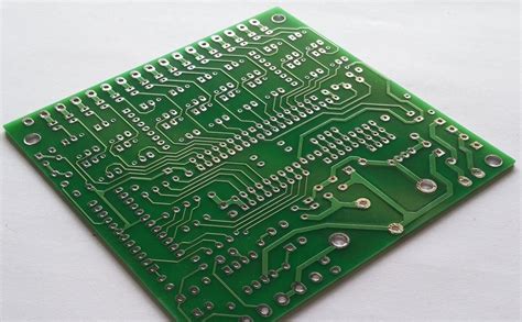
Modern PCB assembly processes achieve peak performance through strategic integration of automation technologies and precision engineering. At the core of PCBA efficiency lies high-speed component placement systems, which ensure microscopic accuracy while reducing human error. Advanced reflow soldering techniques paired with nitrogen-enriched environments eliminate defects like tombstoning or bridging, directly boosting yield rates. The adoption of automated optical inspection (AOI) systems acts as a critical safeguard, scanning boards at micron-level resolution to catch anomalies before final testing.
To optimize throughput, manufacturers deploy smart process controls—such as dynamic line balancing and real-time thermal profiling—that adapt to varying PCB assembly demands. Key metrics like cycle time reduction and first-pass yield are prioritized, ensuring seamless transitions between PCBA stages. By harmonizing these elements, production lines achieve near-zero defect rates while maintaining scalability for high-volume orders. This holistic approach not only accelerates output but also establishes a foundation for continuous improvement in precision-driven manufacturing ecosystems.
SMT Assembly Automation for Peak Performance
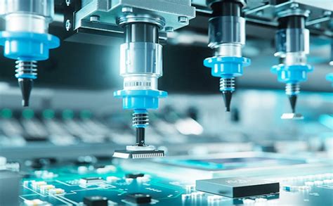
Modern PCB assembly workflows achieve peak performance through intelligent automation that synchronizes high-speed machinery with precision control systems. At the core of PCBA automation are robotic pick-and-place units capable of positioning surface-mount devices (SMDs) at rates exceeding 50,000 components per hour, while maintaining placement accuracies within ±25μm. These systems integrate adaptive vision alignment and real-time feedback loops to compensate for thermal expansion or feeder tape variances, ensuring consistent quality across production batches.
Advanced conveyor systems with closed-loop synchronization eliminate bottlenecks by dynamically adjusting transport speeds to match stencil printing and reflow oven cycles. This harmonization reduces idle time by 22–35% in typical PCB assembly lines. For PCBA applications requiring mixed-technology boards, hybrid automation platforms seamlessly handle both SMDs and through-hole components through programmable tool-switching mechanisms.
Critical to sustaining peak output is the integration of machine learning algorithms that predict maintenance needs for critical components like nozzles and vacuum pumps. By analyzing historical performance data, these systems preemptively flag wear patterns, cutting unplanned downtime by up to 40%. Such automation not only accelerates throughput but also creates a foundation for zero-defect manufacturing when paired with inline inspection protocols – a prerequisite for the subsequent precision placement processes detailed in the next section.
Precision Component Placement in SMT Lines
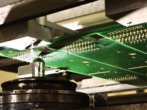
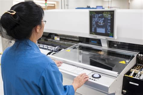
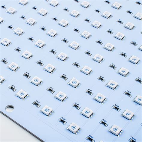
Achieving micrometer-level accuracy in PCB assembly hinges on sophisticated placement systems that balance speed and precision. Modern PCBA lines utilize high-speed pick-and-place machines equipped with vision-guided robotics to position components as small as 01005 packages (0.4 mm x 0.2 mm) at rates exceeding 50,000 placements per hour. These systems rely on real-time feedback loops to adjust for thermal expansion, board warping, and feeder tape inconsistencies, ensuring ±25-micron placement tolerances even in high-mix production environments.
Pro Tip: Regular calibration of nozzle changers and feeder alignment is critical—even a 0.1° angular deviation in chip shooters can cause tombstoning defects in 0201 resistors.
Advanced PCB assembly workflows now integrate machine learning algorithms that analyze historical placement data to optimize nozzle selection and component sequencing. This reduces non-value-added motion by up to 18% in complex PCBA projects while maintaining 99.98% first-pass placement accuracy. Dual-lane conveyor systems further enhance throughput by allowing simultaneous loading/unloading of panels without interrupting the placement cycle, a key advantage for automotive-grade electronics manufacturing. By combining servo-driven actuators with multi-spectral inspection cameras, manufacturers achieve defect rates below 50 ppm while operating at full SMT line capacity.
Advanced Soldering Techniques for Zero Defects
Modern PCB assembly processes demand meticulous control over soldering parameters to eliminate defects in PCBA manufacturing. Reflow soldering remains a cornerstone, but its effectiveness hinges on precise temperature profiling tailored to component thermal tolerances. Advanced systems now integrate real-time thermal monitoring to maintain optimal heat distribution, preventing tombstoning or cold joints. For high-density boards, laser soldering offers micron-level accuracy, particularly for 0201 or 01005 packages where traditional methods struggle.
The adoption of nitrogen-inerted reflow ovens reduces oxidation, enhancing joint reliability while enabling finer-pitch soldering. Pairing this with solder paste inspection (SPI) systems ensures consistent deposition volumes, addressing issues like bridging or insufficient solder before reflow. For hybrid assemblies combining SMT and through-hole components, selective soldering tools target specific areas without affecting adjacent parts, preserving PCB assembly integrity.
Emerging techniques like vapor phase soldering provide uniform heat transfer for thermal-sensitive components, minimizing warping in multilayer PCBA. Post-soldering, automated optical inspection (AOI) cross-references results with SPI data to identify subtle defects invisible to manual checks. By synchronizing these technologies, manufacturers achieve near-zero defect rates while maintaining throughput—a critical balance in high-mix, high-volume PCB assembly environments.
AOI Systems Revolutionizing PCB Production
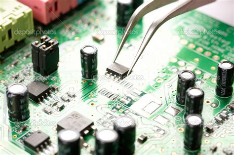
Modern PCB assembly processes now integrate automated optical inspection (AOI) systems as a cornerstone of quality assurance. These systems employ high-resolution cameras, machine vision algorithms, and AI-driven analytics to scrutinize PCBA boards at micron-level precision, identifying defects such as solder bridging, misaligned components, or missing parts in real time. By scanning boards post-reflow and pre-final testing, AOI reduces human error rates by over 70%, ensuring defects are caught before downstream processes amplify their impact.
A critical advantage lies in AOI’s ability to adapt to evolving SMT assembly standards. For instance, systems now correlate inspection data with process parameters—such as stencil thickness or reflow profiles—to pinpoint root causes of defects. This feedback loop enables rapid adjustments, slashing rework cycles by up to 40%. The table below illustrates common defects detected by AOI and their resolution rates:
| Defect Type | Detection Rate | Typical Resolution Time |
|---|---|---|
| Solder Bridging | 98.5% | <15 minutes |
| Component Misalignment | 99.2% | <10 minutes |
| Insufficient Solder Paste | 97.8% | <20 minutes |
Furthermore, AOI systems seamlessly integrate with smart factory ecosystems, feeding data into centralized dashboards for predictive maintenance and process optimization. As PCBA designs grow denser with miniaturized components, the role of AOI in maintaining first-pass yield becomes indispensable. By pairing these systems with design-for-manufacturing (DFM) principles, manufacturers achieve tighter tolerances and faster time-to-market—key drivers in today’s high-mix, low-volume production landscape.
Optimizing SMT Throughput With Smart Processes
Modern PCB assembly workflows achieve peak efficiency through intelligent integration of process monitoring and adaptive control systems. By deploying real-time data analytics across SMT lines, manufacturers gain granular visibility into cycle times, material utilization, and equipment performance. This enables dynamic adjustments to PCBA parameters—such as conveyor speed, nozzle selection, and reflow profiles—to maintain optimal throughput without compromising precision.
Central to this approach are machine learning algorithms that analyze historical production data to predict bottlenecks. For instance, adaptive feeders automatically recalibrate component placement sequences based on detected variances in tape reel tension or part orientation. Simultaneously, closed-loop feedback from AOI systems ensures immediate correction of placement offsets, reducing rework cycles by up to 40%.
Smart scheduling tools further enhance productivity by synchronizing stencil cleaning intervals with board changeovers, minimizing idle time. When paired with modular SMT platforms, these strategies allow seamless scaling from prototype batches to high-volume runs. The result? A 15–25% improvement in line utilization for PCB assembly projects, validated through ISO-certified yield audits.
By unifying automation with data-driven decision-making, manufacturers transform rigid production lines into agile ecosystems capable of meeting fluctuating demand while sustaining sub-100 ppm defect rates.
Minimizing Defects in High-Speed SMT Assembly
Achieving defect-free outcomes in high-speed PCB assembly requires meticulous attention to process variables and equipment calibration. Modern SMT lines employ real-time monitoring of solder paste deposition and component alignment, critical factors influencing yield rates in PCBA manufacturing. Advanced stencil printing systems with laser-cut apertures ensure consistent paste volume, while vision-guided pick-and-place machines maintain ±25μm placement accuracy even at 50,000 components per hour.
The integration of inline inspection technologies creates multiple quality checkpoints. 3D SPI (Solder Paste Inspection) scanners detect insufficient or bridged deposits before reflow, reducing downstream rework by up to 70%. Post-reflow, automated optical inspection (AOI) systems with spectral analysis identify micro-defects like tombstoning or insufficient wetting, achieving detection rates exceeding 99.5% for critical PCB assembly errors.
Process optimization extends to thermal management strategies. Precise reflow oven profiling, adjusted for specific component thermal mass variations, prevents solder balling or cold joints. For PCBA designs with mixed-component densities, adaptive conveyor speed control maintains optimal heat distribution across all board zones. Implementing closed-loop feedback between inspection data and placement machines enables self-correcting assembly lines, where defect patterns trigger immediate parameter adjustments—a key differentiator in high-mix production environments.
Key Strategies for High-Yield SMT Manufacturing
Central to achieving high-yield PCB assembly is the integration of precision machinery with intelligent process controls. Modern PCBA lines combine automated pick-and-place systems with laser-aligned vision technology to achieve micron-level placement accuracy, critical for handling miniaturized components. Implementing real-time thermal profiling during reflow soldering ensures optimal solder joint formation, while nitrogen-enriched environments minimize oxidation risks. For process validation, automated optical inspection (AOI) systems perform 3D solder paste measurement and component alignment checks at speeds exceeding 25,000 inspections/hour.
Yield optimization requires balancing machine capabilities with material science – from selecting low-voiding solder pastes to implementing moisture-sensitive component baking protocols. Advanced PCBA facilities employ closed-loop feedback systems where AOI data directly adjusts placement parameters, creating self-optimizing production lines. Maintaining <500 ppm defect rates demands cross-functional collaboration between design engineers and manufacturing teams to implement design for assembly (DFA) principles from the earliest product development stages.
Leveraging Automation for Flawless SMT Output
Modern PCB assembly workflows demand uncompromising precision to meet the rigorous quality standards of today’s electronics industry. By integrating automated systems into SMT lines, manufacturers achieve repeatable accuracy in component placement, soldering, and inspection—critical for high-volume PCBA production. Robotic pick-and-place machines, for instance, operate at micron-level tolerances, ensuring components like 0201 resistors or QFN packages align perfectly with pad geometries. This eliminates human error while maintaining speeds exceeding 40,000 placements per hour.
Automated solder paste dispensers further enhance reliability by applying consistent volumes across even the densest PCB assembly layouts, preventing defects like bridging or cold joints. Closed-loop feedback mechanisms adjust parameters in real time, compensating for environmental variables such as temperature fluctuations. When paired with intelligent conveyor systems, these technologies create seamless workflows that reduce idle time between processes.
The synergy between automation and PCBA quality control is particularly evident in inline AOI systems, which scan boards at production-line speeds. By cross-referencing defect databases and CAD models, these systems flag anomalies with sub-millimeter precision, enabling immediate corrections. Such integration not only slashes rework costs but also aligns with zero-tolerance standards for aerospace, medical, and automotive applications. As factories adopt modular automation platforms, scalability becomes a strategic advantage, allowing rapid adaptation to evolving SMT technologies without overhauling entire lines.
Conclusion
The evolution of PCB assembly processes underscores the critical role of precision and automation in achieving high-yield PCBA manufacturing. By integrating smart process controls with surface-mount technology (SMT), manufacturers can systematically reduce defects while maintaining throughput in high-speed production environments. The strategic deployment of automated optical inspection (AOI) systems ensures rigorous quality checks, catching deviations that might otherwise compromise final product reliability.
To sustain competitive advantage, optimizing SMT assembly workflows demands a balance between advanced soldering methodologies and real-time data analytics. This synergy not only enhances traceability but also refines component placement accuracy, particularly for miniaturized or complex designs. Collaboration between design engineers and PCBA technicians remains pivotal, as even minor layout adjustments can significantly impact manufacturability and defect rates.
Ultimately, the path to flawless PCB assembly lies in continuous improvement cycles—leveraging feedback from AOI systems, refining material handling protocols, and adopting adaptive automation. These steps ensure that process optimization becomes an ingrained practice, driving both quality and scalability in modern electronics manufacturing.
Frequently Asked Questions
What distinguishes high-performance SMT assembly from conventional methods?
Modern PCB assembly integrates automated optical inspection (AOI) and precision pick-and-place systems, reducing human error by 60-80%. Unlike manual processes, PCBA workflows leverage real-time data analytics to optimize solder paste application and component alignment.
How do AOI systems minimize defects in high-speed production?
AOI cameras scan PCB assembly lines at micron-level resolution, identifying solder bridging, misaligned components, or insufficient paste volumes. These systems flag defects before reflow soldering, preventing costly rework and ensuring PCBA yields exceed 99.5% in optimized setups.
Can automation improve throughput without compromising quality?
Yes. Robotic placement systems achieve 25,000+ components per hour with ±15μm accuracy, while closed-loop thermal profiling maintains consistent reflow conditions. This synergy between speed and precision allows PCBA manufacturers to scale output while keeping defect rates below 50ppm.
What role does solder paste chemistry play in SMT reliability?
Advanced no-clean formulations with Type 4/5 powder sizes create self-centering solder joints during reflow. Paired with nitrogen-assisted ovens, these pastes reduce voiding to <5% in PCB assembly, critical for aerospace and medical-grade applications.
Ready to Elevate Your SMT Production?
For tailored PCB assembly solutions integrating AOI, precision placement, and zero-defect soldering, please click here to consult with our PCBA engineering team.