Suppressing the source of electromagnetic interference in electronic equipment
Electromagnetic interference is widely present in various types of electronic and electrical equipment. Various electronic and electrical equipment will more or less emit electromagnetic waves when working, which will interfere with the normal operation of the entire equipment. In the design of electronic products, due to insufficient consideration of electromagnetic compatibility, some electrical and electronic products are unqualified. Therefore, the author summarizes some key points that should be paid attention to on this issue.
1 Ground connection
Analog and digital circuits have independent power and ground paths. Try to widen the power and ground of these two parts of the circuit, or use separate power layers and ground layers to reduce the impedance of the power and ground loops and reduce any interference voltage that may be in the power and ground loops.
The analog ground and digital ground of the PCB working separately can be connected at a single point near the system grounding point. If the power supply voltage is consistent, the power supply of the analog and digital circuits can be connected at a single point at the power supply entrance. If the power supply voltage is inconsistent, a capacitor of -1 to 2μf is connected near the two power supplies to provide a path for the signal return current between the two power supplies.
The ideal ground wire is a physical entity with zero impedance and zero potential. It is not only the reference point of the signal, but also does not generate voltage drop when current flows through it. In actual electrical and electronic equipment, this ideal ground wire does not exist. When current flows through the ground wire, voltage drop will inevitably occur. Based on this, the interference formation mechanism in the ground wire can be summarized into the following two points: first, reduce low impedance and power feeder impedance. Second, correctly select the grounding method and block the ground loop. According to the grounding method, there are floating ground, single-point ground, multi-point ground, and mixed ground. If the interference of the sensitive line mainly comes from the external space or the system shell, the floating ground method can be used to solve it. However, the floating ground device is prone to static electricity accumulation. When the charge reaches a certain level, static electricity discharge will occur. Therefore, the floating ground is not suitable for general electronic equipment.
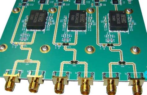
2 PCB component layout requirements
The layout of circuit elements and signal paths must minimize the mutual coupling of useless signals:
(1) Low-level signal channels cannot be close to high-level signal channels and unfiltered power lines, including circuits that can generate transient processes.
(2) High, medium and low speed logic circuits should use different areas on the PCB.
(3) When arranging the circuit, the length of the signal line should be minimized.
(4) Ensure that there are no long parallel signal lines between adjacent boards, between adjacent layers of the same board, and between adjacent wiring on the same layer.
(5) The electromagnetic interference (EMI) filter should be as close to the EMI source as possible and placed on the same circuit board.
(6) The DC/DC converter, switching elements and rectifier should be placed as close to the transformer as possible to minimize the length of their wires.
(7) Place the voltage regulator and filter capacitor as close to the rectifier diode as possible.
(8) The printed circuit board is divided into zones according to frequency and current switching characteristics, and the noise elements and non-noise elements should be farther apart.
(9) Noise-sensitive wiring should not be parallel to high current and high-speed switching lines.
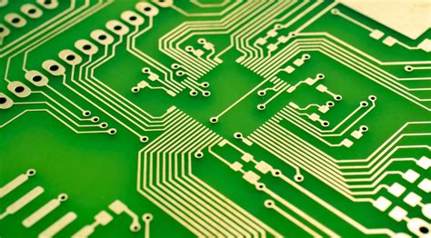
3 Multilayer board design
In the multilayer board design, the power plane should be close to the ground plane and arranged below the ground plane. In this way, the capacitor between the two metal plates can be used as a smoothing capacitor for the power supply. At the same time, the ground plane also shields the radiation current distributed on the power plane. In order to produce flux cancellation, the wiring layer should be arranged adjacent to the entire metal plane. The printed lines in the middle layer form a planar waveguide and the microstrip lines on the surface. The transmission characteristics of the two are different. The clock circuit and high-frequency circuit are the main sources of interference and radiation. They must be arranged separately and away from sensitive circuits. All printed boards with a certain voltage will radiate electromagnetic energy into space. To reduce this effect, the physical size of the printed board should be 20H smaller than the physical size of the closest ground plane, where H is the distance between the two printed board surfaces. According to the typical printed board size, 20H is generally about 3mm.
To avoid electromagnetic crosstalk caused by the small spacing between two printed lines, any line spacing should be kept not less than 2 times the width of the printed line, that is, not less than 2W, where w is the width of the printed line.
3.1 Setting decoupling capacitors
Good high-frequency decoupling capacitors can remove high-frequency components as high as 1GHZ. Ceramic chip capacitors or multilayer ceramic capacitors have better high-frequency characteristics. When designing a printed circuit board, a decoupling capacitor should be added between the power supply and ground of each integrated circuit. The decoupling capacitor has two functions: on the one hand, it is the energy storage capacitor of the integrated circuit, providing and absorbing the charging and discharging energy of the integrated circuit when opening and closing the door; on the other hand, it bypasses the high-frequency noise of the device.
3.2 Suppress electromagnetic coupling between lines
Reduce the loop area of interference sources and sensitive circuits. The best way is to use twisted pair and shielded wires, twist the signal line and the ground line (or current-carrying loop) together to minimize the distance between the signal and the ground line (or current-carrying loop); increase the distance between the lines to minimize the mutual inductance between the interference source and the induced line; if possible, make the interference source line and the induced line at right angles (or close to right angles), which can greatly reduce the coupling between the two lines;
3.3 Other methods to reduce noise and electromagnetic interference
(1) Use ground wire to circle the clock area, and keep the clock line as short as possible.
(2) Try to provide some form of damping for relays, etc.
(3) Use the lowest frequency clock that meets the system requirements.
(4) The clock generator should be as close as possible to the device that uses the clock. The quartz crystal oscillator housing should be grounded.
(5) The I/O drive circuit should be as close as possible to the edge of the printed circuit board to allow it to leave the printed circuit board as soon as possible. The signals entering the printed circuit board should be filtered, and the signals coming from the high noise area should also be filtered. At the same time, use the method of series terminal resistance to reduce signal reflection.
(6) The input terminals of unused gate circuits should not be left floating. The positive input terminals of unused op amps should be grounded, and the negative input terminals should be connected to the output terminals.
(7) The printed circuit board should use 45-degree fold lines instead of 90-degree fold lines as much as possible to reduce the external emission and coupling of high-frequency signals.
(8) The clock, bus, and chip select signals should be kept away from the I/O lines and connectors.
(9) The analog voltage input line and the reference voltage terminal should be kept away from the digital circuit signal lines, especially the clock.
For A/D devices, the digital part and the analog part should be unified rather than crossed.
(10) Do not route under quartz crystals or noise-sensitive devices.
4 Conclusion
In PCB design, the impact of various interferences must be taken into consideration. A complete design can effectively simulate electromagnetic interference, shorten product design cycles, and improve system stability and reliability.


