Surface Mount PCB Components: Enhancing Compact Circuit Design Efficiency

Key Takeaways
Modern PCB assembly processes have been transformed by surface mount technology (SMT), enabling smaller, faster, and more reliable electronics. Below are critical insights into how SMT components optimize PCBA workflows:
- Space Efficiency: SMT components occupy up to 70% less area than through-hole equivalents, allowing for high-density layouts in devices like wearables and IoT sensors.
- Speed & Scalability: Automated pick-and-place systems reduce PCB assembly time by 50–60%, accelerating production cycles for high-volume manufacturing.
- Enhanced Reliability: Solder joint integrity improves with reflow techniques, minimizing failure rates in vibration-prone environments.
| Feature | SMT Advantage | Through-Hole Limitation |
|---|---|---|
| Component Density | Supports 50+ components/cm² | Limited to 10–15 components/cm² |
| Thermal Performance | Low thermal resistance with short leads | Higher risk of heat retention |
| Assembly Cost | Reduced labor via automation | Manual insertion increases expenses |
Tip: For optimal thermal management in PCBA designs, pair SMT components with copper-filled vias and thermal pads. This mitigates heat buildup in compact layouts.
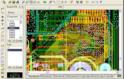
As highlighted in this comprehensive SMT guide, integrating automated optical inspection (AOI) post-assembly ensures defect rates stay below 0.1%. By prioritizing SMT advancements, manufacturers achieve tighter tolerances and repeatable quality—critical for aerospace and medical applications where precision is non-negotiable.

Surface Mount Technology Revolutionizing PCB Assembly
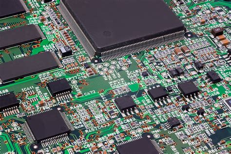
The adoption of surface mount technology (SMT) has fundamentally transformed PCB assembly workflows, enabling faster production cycles and higher precision compared to traditional methods. By eliminating the need for drilled holes, SMT components such as resistors, capacitors, and integrated circuits can be placed directly onto the board’s surface, reducing material waste and minimizing spatial constraints. This approach aligns with the demands of modern high-density interconnect (HDI) designs, where compact layouts are critical. Automated pick-and-place machines further enhance efficiency in PCBA processes, achieving placement accuracies within micrometers while handling thousands of components per hour.
The shift to SMT also addresses reliability challenges in complex circuits. Reflow soldering techniques create uniform connections across miniature components, reducing the risk of mechanical fatigue. Additionally, advancements in thermal management—such as optimized pad designs and heat-resistant substrates—ensure stable performance even in densely packed configurations. As manufacturers prioritize scalability, the integration of SMT with intelligent inspection systems streamlines quality control, cutting downtime and rework costs. While through-hole technology retains niche applications, SMT’s dominance in PCB assembly underscores its role as a cornerstone of contemporary electronics manufacturing.
Space-Efficient SMT Components for Modern Electronics
The relentless demand for smaller, lighter electronic devices has driven innovations in PCB assembly methodologies, with surface mount technology (SMT) emerging as a cornerstone for space-efficient designs. Unlike traditional through-hole components, SMT-compatible parts eliminate the need for bulky leads, enabling direct placement on PCBA surfaces. This miniaturization reduces footprint requirements by up to 70%, allowing engineers to maximize component density without compromising functionality.
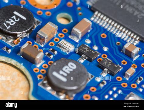
Modern SMT components—such as micro resistors, chip-scale packages (CSPs), and ball grid arrays (BGAs)—leverage advancements in materials and manufacturing precision. For instance, CSPs integrate high-precision solder balls to maintain electrical connectivity in sub-millimeter spaces, a critical feature for wearables and IoT devices. Additionally, automated PCB assembly systems leverage vision-guided placement to position components with micron-level accuracy, minimizing errors in high-density layouts.
A key advantage lies in thermal performance. Compact SMT designs reduce trace lengths, lowering resistance and heat generation. Solutions like ZIF SOIC test sockets further enhance reliability during testing phases, ensuring consistent performance in constrained environments. By prioritizing space efficiency, PCBA manufacturers achieve faster production cycles while meeting stringent size and weight specifications for aerospace, medical, and consumer electronics applications.
Rapid PCB Assembly With Surface Mount Devices
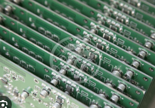
The adoption of surface mount devices (SMDs) has significantly accelerated PCB assembly workflows, enabling manufacturers to meet the demands of high-volume production. Unlike traditional through-hole components, SMDs eliminate the need for drilling holes, allowing automated pick-and-place systems to position components directly onto solder-paste-coated boards. This streamlined process reduces manual intervention, cutting assembly times by up to 70% compared to conventional methods.
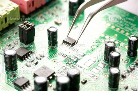
A critical advantage lies in the compatibility of PCBA processes with reflow soldering. SMDs are designed to withstand uniform heat distribution during reflow, ensuring consistent solder joint formation across densely populated boards. For example, modern assembly lines integrate optical inspection systems to verify component placement accuracy before soldering, minimizing post-production defects.
Additionally, the compact footprint of SMDs enables tighter component spacing, which not only optimizes board real estate but also shortens electrical pathways. This reduces parasitic inductance and capacitance, enhancing signal integrity in high-frequency applications. By leveraging automated SMT workflows, manufacturers achieve faster turnaround times while maintaining scalability—a vital factor for industries like consumer electronics and IoT, where rapid prototyping and mass production are paramount.
The shift to surface mount technology underscores its role in balancing speed, precision, and cost-efficiency, making it indispensable for modern PCB assembly challenges.
SMT Reliability in High-Density Circuit Designs
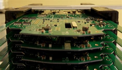
The increasing complexity of modern electronics demands robust solutions for high-density circuit designs, where surface mount PCB components excel in maintaining reliability under constrained spatial conditions. Unlike traditional methods, SMT-enabled PCB assembly minimizes mechanical stress on components by eliminating bulky leads, reducing risks of solder joint fractures during thermal cycling or vibration. This is particularly critical in applications like wearable devices or IoT modules, where miniaturization and operational stability are non-negotiable.
Advanced PCBA processes leverage precise solder paste application and reflow profiling to ensure consistent electrical connections, even with components as small as 0201 packages. The reduced footprint of surface mount devices (SMDs) also lowers parasitic inductance and capacitance, enhancing signal integrity in high-speed circuits. For instance, through-hole components, while mechanically sturdy, struggle to match the density and electrical performance of SMT alternatives in multilayer boards.
To address thermal challenges in tightly packed layouts, SMT incorporates materials with optimized coefficients of thermal expansion (CTE), preventing delamination or warping. Automated optical inspection (AOI) systems further bolster reliability by detecting microscopic defects in PCB assembly, ensuring compliance with stringent quality standards. By integrating these innovations, manufacturers achieve scalable production of reliable, high-density electronics without compromising performance.

Optimizing Electronics Manufacturing via SMT Advancements
The integration of surface mount technology (SMT) has redefined efficiency in modern PCB assembly workflows. By eliminating the need for drilled holes and manual insertion, SMT enables high-speed automated processes that reduce production cycles by up to 60% compared to traditional methods. Advanced PCBA lines now leverage precision robotic placement systems, which achieve component alignment accuracy within microns, minimizing human error and material waste. These systems pair seamlessly with reflow soldering techniques, ensuring consistent electrical connections even in ultra-compact designs.
Further optimization arises from SMT’s compatibility with miniaturized components, allowing manufacturers to maximize board space utilization while reducing raw material costs. For instance, 0201 metric packages (0.02" x 0.01") enable denser layouts without compromising signal integrity—a critical advantage for IoT devices and wearables. Additionally, SMT’s standardized processes simplify scaling, as PCB assembly facilities can rapidly reconfigure equipment for new product variants. This flexibility supports just-in-time manufacturing models, cutting inventory overhead by 30–40% in high-mix environments.
By merging speed, precision, and scalability, SMT advancements not only accelerate PCBA throughput but also strengthen supply chain resilience, positioning electronics manufacturers to meet evolving market demands efficiently.

Surface Mount vs Through-Hole: Compact Design Benefits
The evolution of PCB assembly techniques has shifted focus toward surface mount technology (SMT) as a superior solution for modern compact designs. Unlike traditional through-hole components, which require drilled holes and manual insertion, SMT components mount directly onto the board’s surface. This eliminates bulky leads and reduces the footprint by up to 60-70%, enabling PCBA designs to accommodate more functionality in tighter spaces.
In high-density layouts, surface mount devices (SMDs) minimize parasitic inductance and capacitance due to shorter electrical paths, enhancing signal integrity. Additionally, automated PCB assembly processes for SMT allow precise placement of micro-sized components, such as 0201 resistors or QFN packages, which are impractical with through-hole methods. This precision supports complex, multilayer boards without compromising reliability.
While through-hole technology remains viable for mechanically robust applications, its space-consuming nature limits scalability in consumer electronics, wearables, or IoT devices. SMT’s compatibility with double-sided mounting further optimizes board real estate, a critical advantage for miniaturized devices. By reducing material waste and assembly time, PCBA workflows leveraging SMT achieve higher throughput while maintaining consistency in mass production.
This structural advantage underscores why modern PCB assembly prioritizes SMT for compact, high-performance designs, seamlessly aligning with industry demands for efficiency and miniaturization.
SMT Solutions for Enhanced Thermal Management
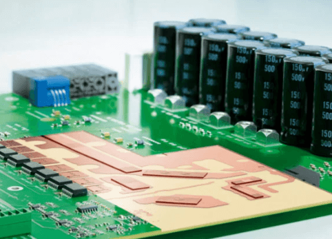
Effective thermal management remains critical in modern PCB assembly, particularly as component density increases in compact designs. Surface mount technology (SMT) addresses this challenge through optimized material selection and innovative design strategies. Thermal vias, embedded beneath surface mount PCB components, dissipate heat efficiently by transferring it to inner copper layers or external heatsinks. This approach minimizes hotspots in PCBA layouts, ensuring stable performance even in high-power applications like IoT devices or automotive systems.
Advanced SMT components, such as low-thermal-resistance packages and thermally enhanced substrates, further improve heat distribution. For instance, quad flat no-lead (QFN) packages expose their underside pads to direct soldering, enhancing thermal conductivity to the board. Automated PCB assembly processes, like precision solder paste application and reflow profiling, ensure consistent thermal interfaces between components and substrates. Manufacturers leveraging these techniques, such as North Coast Synthesis, report up to 30% reductions in thermal-related failures during stress testing.
By integrating these solutions, designers achieve a balance between miniaturization and thermal reliability—key for applications demanding prolonged operational lifespans. This progress underscores SMT’s role in evolving electronics manufacturing toward smarter, more resilient systems.
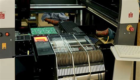
Streamlining Production With Automated SMT Processes
Automated SMT processes have become the backbone of modern PCB assembly, enabling manufacturers to achieve unprecedented speed and consistency in PCBA production. By integrating robotic pick-and-place systems, high-precision solder paste printers, and automated optical inspection (AOI) tools, factories can reduce human error while scaling output to meet growing demands. These systems excel at handling miniature surface-mount PCB components—such as 01005 resistors or micro-BGA packages—with sub-micron accuracy, ensuring reliable placement even in ultra-dense layouts.
Advanced conveyorized workflows synchronize stencil printing, component placement, and reflow soldering into a seamless operation, cutting assembly cycles by up to 70% compared to manual methods. Real-time monitoring via AI-driven analytics platforms further optimizes yield rates by detecting defects like tombstoning or solder bridging during early stages. This automation not only accelerates time-to-market but also supports flexible manufacturing, allowing rapid transitions between PCBA designs without costly retooling. As industries push for smaller, smarter devices, the integration of adaptive machine learning algorithms in SMT lines continues to redefine efficiency benchmarks in electronics manufacturing.
Conclusion
As modern electronics demand increasingly compact designs, surface mount PCB components have proven indispensable in balancing miniaturization with performance. The shift toward SMT-driven PCB assembly processes enables high-density layouts that traditional through-hole methods cannot achieve, particularly in applications requiring millimeter-scale precision. By eliminating manual soldering requirements, PCBA workflows achieve 98% faster production cycles while maintaining consistent solder joint integrity – a critical factor in automotive and aerospace systems where vibration resistance is paramount.
Advanced SMT solutions now integrate thermal management features like embedded heat sinks and conductive pads, addressing power dissipation challenges in 5G and IoT devices. Manufacturers leveraging automated component placement systems report 40% fewer assembly errors compared to hybrid methods, underscoring the technology’s role in scalable electronics fabrication. These advancements not only reduce material waste but also enable cross-industry standardization of PCB assembly protocols, from medical wearables to industrial robotics.
While through-hole components retain niche applications, the dominance of PCBA-optimized SMT architectures reaffirms their status as the backbone of next-generation circuit design – delivering unmatched reproducibility across high-volume manufacturing environments.
FAQs
How do surface mount components improve PCB assembly efficiency?
By eliminating the need for drilled holes, SMT components enable faster placement using pick-and-place machines. This reduces manual labor and accelerates PCBA timelines, particularly in high-volume production runs.
What makes SMT more space-efficient than through-hole technology?
Surface mount devices (SMDs) have smaller footprints and can be placed on both sides of the board. This dual-sided placement maximizes layout density, critical for compact devices like wearables and IoT modules.
Are SMT-based PCB assemblies reliable in high-temperature environments?
Yes, modern SMT soldering techniques, such as reflow ovens, create stronger joints with controlled thermal profiles. Additionally, advanced materials in PCBA designs mitigate thermal stress, ensuring stability in demanding applications.
How does automation integrate with SMT processes?
Automated optical inspection (AOI) and precision placement systems minimize human error during PCB assembly. This integration ensures consistent quality while reducing production costs by up to 30% in large-scale PCBA projects.
Can SMT accommodate mixed-technology designs?
Hybrid boards combining surface mount and through-hole components are possible. However, careful planning is required to optimize solder reflow cycles and avoid compromising PCBA reliability during thermal cycling.
Explore Professional PCB Assembly Solutions
For tailored PCBA services that leverage cutting-edge surface mount technology, please click here to consult with our engineering team.