Sustainable PCB Design: Principles, Practices, and Future Directions
Introduction
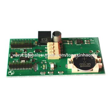
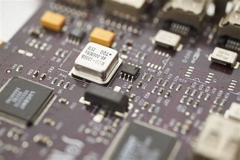
Printed Circuit Boards (PCBs) are the backbone of modern electronics, found in everything from smartphones to industrial machinery. However, the environmental impact of PCB manufacturing and disposal is significant, contributing to electronic waste (e-waste), toxic pollution, and resource depletion. Sustainable PCB design aims to mitigate these impacts by incorporating eco-friendly materials, energy-efficient processes, and end-of-life recyclability.
This article explores the key principles of sustainable PCB design, current best practices, challenges, and future innovations that can help the electronics industry transition toward a greener future.
1. The Environmental Impact of Traditional PCBs
Before discussing sustainable alternatives, it is essential to understand the environmental drawbacks of conventional PCB manufacturing:
1.1 Toxic Materials
Traditional PCBs contain hazardous substances such as:
- Lead (Pb) – Used in solder, poses health and environmental risks.
- Brominated Flame Retardants (BFRs) – Found in laminates, linked to bioaccumulation and toxicity.
- Heavy Metals (Cadmium, Mercury, Hexavalent Chromium) – Used in plating and coatings, harmful if leached into soil and water.
1.2 Energy-Intensive Manufacturing
PCB fabrication involves high-energy processes like:
- Etching – Uses chemicals (e.g., ferric chloride) that require disposal.
- Plating – Involves electrolysis, consuming significant electricity.
- Lamination – Requires high heat and pressure.
1.3 E-Waste and Non-Recyclability
Millions of discarded PCBs end up in landfills annually due to:
- Complex Material Composition – Difficult to separate and recycle.
- Short Product Lifecycles – Rapid technological obsolescence increases waste.
Given these challenges, sustainable PCB design is critical for reducing the electronics industry’s ecological footprint.
2. Principles of Sustainable PCB Design
Sustainable PCB design follows three core principles:
2.1 Material Selection
Choosing eco-friendly materials reduces toxicity and improves recyclability:
- Lead-Free Solder – Alternatives like SAC (Sn-Ag-Cu) alloys comply with RoHS regulations.
- Halogen-Free Substrates – Replace BFRs with phosphorus-based or inorganic flame retardants.
- Biodegradable Substrates – Research into bio-based resins (e.g., flax, hemp fibers) is ongoing.
2.2 Energy-Efficient Manufacturing
Reducing energy consumption in PCB production involves:
- Additive Manufacturing – 3D printing PCBs minimizes material waste.
- Dry Processes – Using laser etching instead of chemical etching.
- Renewable Energy – Powering factories with solar or wind energy.
2.3 Design for Recyclability (DfR)
Improving PCB recyclability requires:
- Modular Design – Easier disassembly for component reuse.
- Standardized Materials – Reducing mixed-material layers for easier separation.
- Marking for Recycling – Labeling materials to aid automated sorting.
3. Best Practices in Sustainable PCB Design
Several strategies can be implemented today to enhance sustainability:
3.1 Minimizing PCB Size and Layers
- Smaller PCBs use fewer materials and reduce waste.
- Optimized layer stacking decreases raw material consumption.
3.2 Using Recycled and Recyclable Materials
- Recycled copper and reclaimed laminate materials lower environmental impact.
- Designing for easy metal recovery (e.g., gold, silver) improves recycling efficiency.
3.3 Reducing Hazardous Chemicals
- Adopting water-based fluxes instead of VOC-emitting solvents.
- Switching to non-toxic etching agents (e.g., citric acid instead of ammonium persulfate).
3.4 Extending Product Lifespan
- Designing for repairability and upgradability reduces e-waste.
- Implementing robust components to withstand longer usage.
3.5 Implementing Circular Economy Models
- Take-back programs for used PCBs to recover valuable materials.
- Refurbishing and reusing functional PCB components.
4. Challenges in Sustainable PCB Adoption
Despite progress, several barriers hinder widespread sustainable PCB adoption:
4.1 Cost Considerations
- Eco-friendly materials (e.g., halogen-free laminates) are often more expensive.
- Retooling factories for green processes requires significant investment.
4.2 Performance Trade-offs
- Some lead-free solders have higher melting points, affecting reliability.
- Bio-based substrates may lack the durability of traditional FR-4.
4.3 Regulatory and Industry Barriers
- Inconsistent global regulations complicate compliance.
- Slow industry adoption due to entrenched manufacturing practices.
5. Future Innovations in Sustainable PCB Design
Emerging technologies could revolutionize PCB sustainability:
5.1 Biodegradable and Bio-Based PCBs
- Research into fungal mycelium and cellulose-based PCBs shows promise.
- Transient electronics that dissolve after use could reduce e-waste.
5.2 Advanced Recycling Techniques
- Biometallurgy – Using bacteria to extract metals from PCBs.
- Electrochemical Recycling – Efficiently recovering precious metals.
5.3 AI and Machine Learning for Optimization
- AI-driven design tools can minimize material usage while maintaining performance.
- Predictive maintenance extends PCB lifespan.
5.4 Self-Healing PCBs
- Materials that repair minor damage autonomously could reduce replacements.
6. Conclusion
Sustainable PCB design is no longer optional—it is a necessity for reducing the electronics industry’s environmental impact. By adopting eco-friendly materials, energy-efficient processes, and recyclable designs, manufacturers can significantly lower their carbon footprint.
While challenges remain, ongoing innovations in biodegradable materials, advanced recycling, and AI-driven optimization offer a path toward truly sustainable electronics. The transition requires collaboration among designers, manufacturers, policymakers, and consumers to create a circular economy where PCBs are both high-performing and environmentally responsible.


