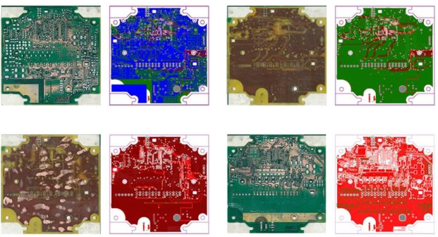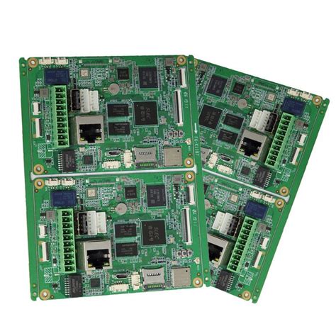
Techniques of Protel software in high-frequency circuit wiring
Digital devices are developing in the direction of high speed, low power consumption, small size and high anti-interference. This development trend has put forward many new requirements for the design of printed circuit boards. The application of Protel software in China has been quite common. However, many designers only focus on the “routing rate” of Protel software. The improvements made to Protel software to adapt to the changes in device characteristics are not used in the design. This not only leads to serious waste of software resources, but also makes it difficult for many new devices to exert their excellent performance. This article intends to introduce the general requirements of high-frequency circuit wiring, and take Protel for Windows V1.5 software as an example to introduce some special countermeasures that Protel software can provide when wiring high-frequency circuits.
(1) High-frequency circuits are often highly integrated and have a large wiring density.
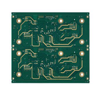
The use of multi-layer boards is both necessary for wiring and an effective means to reduce interference. Protel for Windows V1.5 can provide 16 copper wire layers and 4 power supply layers. Reasonable selection of the number of layers can greatly reduce the size of the printed board, make full use of the middle layer to set the shield, better achieve the nearest grounding, effectively reduce the parasitic inductance, effectively shorten the signal transmission length, and greatly reduce the cross interference between signals, etc. All of these are beneficial to the reliable operation of high-frequency circuits. According to data, when the same material is used, the noise of a four-layer board is 20dB lower than that of a double-layer board. However, the higher the number of board layers, the more complex the manufacturing process and the higher the cost.
(2) The fewer bends in the leads between the pins of high-speed circuit devices, the better.
The leads of high-frequency circuit wiring are preferably all straight lines. If a turn is required, a 45-degree bend line or an arc turn can be used. This requirement is only used to improve the adhesion strength of the steel foil in low-frequency circuits, but in high-frequency circuits, meeting this requirement can reduce the external emission of high-frequency signals and mutual coupling. When routing with Protel, you can make pre-settings in the following two places: one is to make an appointment to route in 45/90 Line or 90 Arc/Line mode in the “Track Mode” submenu of the “Options” menu; the other is to select “Add Arcs” in the “Routing Passes” dialog box opened by the “Setup Autorouter…” item of the “Auto” menu, so that the corners can be rounded at the end of automatic routing.
(3) The shorter the leads between the pins of high-frequency circuit components, the better.
The most effective way for Protel to meet the shortest routing requirement is to make “routing” reservations for individual key high-speed networks before automatic routing. First, open the “Edit Net” submenu of the “Netlst” menu, and a “Change Net” dialog box will appear. Select “Shortest” for “OptimizeMethod (routing optimization mode)” in this dialog box. Second, from an overall perspective, use the “Placement” in “Auto” when placing components. Tools-Shove’ and “Density Check” in “Auto” are used to compare and adjust the arrangement of components to make them compact. In addition, the “Length” function in the “Netlist” menu and the “Length of selection” function in the “Info” menu are used to measure the wiring length of the key network that needs to be minimized.
(4) The fewer the interlayer alternations between the pins of high-frequency circuit components, the better.
The so-called “the fewer interlayer alternations between the leads, the better” means that the fewer vias (Via) used in the component connection process, the better. According to measurements, a via can bring about 0.5 pF of distributed capacitance. Reducing the number of vias can significantly increase the speed. Protel software specifically provides this function. In the “Routing Passes” dialog box opened by the “Setup Autorouter…” item in the Auto menu, there is an “Advanced” column. Set “Smoothing” to on.
(5) When routing high-frequency circuits, attention should be paid to the “cross interference” introduced by the close parallel routing of signal lines.
If parallel distribution cannot be avoided, a large area of ”ground” can be arranged on the opposite side of the parallel signal lines to greatly reduce interference. Parallel routing within the same layer is almost inevitable, but in two adjacent layers, the routing directions must be perpendicular to each other, which is not difficult to do in Protel but is easy to overlook. In the Routing Lagers dialog box opened by the “Setup Autorouter…” item in the “Auto” menu, the routing direction of each layer can be preset. There are three pre-selected directions: “Horizontal, Vertical, and No Preference”. Many users are accustomed to selecting “No Preference”, believing that this will increase the routing rate. However, in high-frequency circuit wiring, it is best to alternate horizontal and vertical wiring in adjacent layers. Parallel routing within the same layer cannot be avoided, but a large area of ground wire can be laid on the back of the printed board to reduce interference (this is for commonly used double-sided boards, and multi-layer boards can use the middle power layer to achieve this function). In the past, Protel software only provided a simple “Fill” function to cope with this demand. Now Protel under Windows also provides a more powerful placement “Polygon” in the “Place” option of the “Edit” menu. Plane” function, that is: polygonal grid (strip) copper foil surface.
If the polygon is taken as a surface of the entire printed board when it is placed, and this grid (strip) is connected to the GND network of the circuit, then this function will be able to realize the “copper plating” operation on a certain side of the entire circuit board. In addition to improving the high-frequency anti-interference ability just mentioned, the “copper plating” circuit board is also very beneficial to heat dissipation and printed board strength. In addition, if tinned grids are added to the fixed parts of the metal chassis of the circuit board, it can not only improve the fixing strength and ensure good contact, but also use the metal chassis to form a suitable common line. After turning on this function in the software menu, you can see a “Place Polygon Plane” dialog box, which will ask you whether you want to connect the placed polygonal grid (strip) to the network (connect net).
If you connect this item, you will be prompted to give the name of the network you want to connect when you exit the dialog box. The given GND network will act as a shielding layer. At the same time, you will be asked whether the “copper plating” pattern is horizontal strips (horizonta), vertical strips (vertica) or grids (both can be selected). The use of a grid will have a better shielding effect. At the same time, the size of the grid (commonly known as “mesh”) is determined according to the interference frequency to be shielded.
(6) Measures to surround particularly important signal lines or local units with ground wires.
This measure can also be automatically implemented in Protel software. It is “Outline Selected Items” under “Place” in the “Edit” menu, that is, drawing the outer contour of the selected object. Using this function, the selected important signal lines can be automatically processed with the so-called “ground wrapping”. Of course, using this function for local ground wrapping of units such as clocks will also be very beneficial to high-speed systems.
(7) All types of signal routing cannot form loops, and ground wires cannot form current loops
. In addition to the shortest principle mentioned above, the routing principles of Protel automatic routing also include routing based on the X direction, based on the Y direction, and daisy-shaped routing. The use of daisy-shaped routing can effectively avoid the formation of loops during routing. Specifically, you can open the “Edit Net” submenu of the “Netlist” menu, and a “Change Net” dialog box will appear. In this dialog box, select “Daisy Chain” for “Optimize Method (wiring optimization mode)”.
(8) A high-frequency decoupling capacitor should be set near each integrated circuit block.
Since Protel software does not consider the positional relationship between the decoupling capacitor and the decoupled integrated circuit when automatically placing components, if the software is allowed to place them, the two will be too far apart, and the decoupling effect will be greatly reduced. At this time, you must manually move the components (“Edit”, ” Move” “component”) method to intervene in the position of the two in advance and make them close.
(9) When analog ground wire, digital ground wire, etc.
are connected to the common ground wire, a high-frequency choke link must be used. When assembling the high-frequency choke link in practice, a high-frequency ferrite bead with a wire passing through the center hole is often used. It is generally not expressed on the circuit schematic, and the resulting network table (netlist) does not include such components, so its existence will be ignored during wiring. In view of this reality, it can be treated as an inductor in the schematic diagram, and a component package can be defined for it separately in the PCB component library. Before wiring, it can be manually moved to a suitable position close to the common ground line junction.