Ten standards for RF PCB
1) In the design of low-power RF PCB, standard FR4 materials (good insulation properties, uniform material, dielectric constant ε=4, 10%) are mainly used.
4-layer to 6-layer boards are mainly used. In the case of very cost-sensitive, double-sided boards with a thickness of less than 1mm can be used. It is necessary to ensure that the back is a complete ground layer. At the same time, since the thickness of the double-sided board is more than 1mm, the FR4 medium between the ground layer and the signal layer is thicker. In order to make the RF signal line impedance reach 50 ohms, the width of the signal line is often about 2mm, making the spatial distribution of the board difficult to control. For a four-layer board, in general, the top layer only carries the RF signal line, the second layer is a complete ground, the third layer is the power supply, and the bottom layer generally carries the digital signal line that controls the state of the RF device (such as setting the clk, data, and LE signal lines of the ADF4360 series PLL.) It is best not to make the power supply of the third layer into a continuous plane, but to make the power supply lines of each RF device distributed in a star shape and finally connected to a point. The power supply traces of the RF devices on the third layer should not cross the digital lines on the bottom layer.
2) For a mixed-signal PCB, the RF part and the analog part should be kept away from the digital part (this distance is usually more than 2cm,
at least 1cm), and the grounding of the digital part should be separated from the RF part.
It is strictly forbidden to use a switching power supply to directly power the RF part. The main reason is that the ripple of the switching power supply will modulate the signal of the RF part.
This modulation often seriously damages the RF signal and leads to fatal results. Usually, the output of the switching power supply can pass through a large choke and a π filter, and then through a linearly regulated low-noise LDO (Micrel’s MIC5207, MIC5265 series, for high-voltage, high-power RF circuits, you can consider using LM1085, LM1083, etc.) to obtain the power supply for the RF circuit.
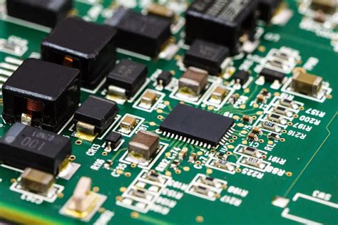
3) In the RF PCB, the components should be arranged closely to ensure that the connection between the components is as short as possible.
For the ADF4360-7 circuit, the distance between the VCO inductor on pin-9 and pin-10 and the ADF4360 chip should be as short as possible to ensure that the distributed series inductance caused by the connection between the inductor and the chip is minimized. For the ground (GND) pins of various RF devices on the board, including the pins of resistors, capacitors, and inductors connected to the ground (GND), vias should be drilled as close to the pins as possible to connect to the ground layer (second layer).
4) When selecting components that work in a high-frequency environment, use surface-mount components as much as possible.
This is because surface-mount components are generally small in size and the pins of the components are very short. This can minimize the impact of additional parameters caused by component pins and internal wiring of components. Especially for discrete resistors, capacitors, and inductors, using smaller packages (0603\0402) is very helpful to improve the stability and consistency of the circuit;
5) Active devices working in high-frequency environments often have more than one power pin.
At this time, it is important to set a separate decoupling capacitor near each power pin (about 1mm), with a capacitance of about 100nF. If the circuit board space allows, it is recommended to use two decoupling capacitors for each pin, with capacitances of 1nF and 100nF respectively. Generally, ceramic capacitors made of X5R or X7R are used. For the same RF active device, different power pins may power different functional parts in the device (chip), and each functional part in the chip may work at different frequencies.
For example, ADF4360 has three power pins, which power the VCO, PFD and digital parts in the chip.
These three parts implement completely different functions and have different operating frequencies. Once the low-frequency noise of the digital part is transmitted to the VCO part through the power line, the VCO output frequency may be modulated by this noise, resulting in spurious noise that is difficult to eliminate. In order to prevent such a situation, in addition to using a separate decoupling capacitor, the power supply pins of each functional part of the active RF device must be connected together through an inductor bead (about 10uH).
This design is very beneficial to the improvement of the isolation performance of LO-RF and LO-IF of active mixers that include LO buffer amplifiers and RF buffer amplifiers.
6) For the input and output of RF signals on the PCB, a special RF coaxial connector must be used.
The most commonly used one is the SMA type connector. For SMA connectors, there are direct plug-in and microstrip types. For signals with frequencies below 3GHz, and the signal power is not large, and we do not care about the weak insertion loss, the direct plug-in SMA connector can be used. If the signal frequency is further increased, we need to carefully select the RF connection wire and RF connector. At this time, the direct plug-in SMA connector may cause relatively large signal insertion loss due to its structure (mainly turning).
At this time, a microstrip SMA connector with better quality (the key is that the connector uses PTFE insulator material) can be used to solve the problem. Similarly, if your frequency is not high, but you are demanding on the indicators of insertion loss, power, etc., you can also consider the microstrip SMA connector. In addition, there are small RF connectors such as SMB and SMC. For SMB connectors, this type of connector generally only supports signal transmission below 2GHz, and the snap-on structure used by SMB connectors will “flash disconnect” in high vibration situations. So you should consider carefully when choosing SMB connectors. Most RF connectors have a 500-time plug-in and pull-out limit. Too frequent plug-in and pull-out may permanently damage the connector, so when debugging the RF circuit, don’t screw the RF connector as a screw. Since the PCB seat of SMB is a pin-type structure (male), frequent plug-in and pull-out will result in relatively small loss of the connector welded on one end of the PCB, reducing the difficulty of maintenance, so in this case, SMB connectors are also a good choice. In addition, for those occasions with extremely high space requirements, there are also micro connectors such as GDR for selection. For analog signals with impedances other than 50 ohms, low frequency, small signal, precision DC, or digital signals such as high-frequency clocks, low-jitter clocks, and high-speed serial signals in the digital part, SMA can be used as a feed-in connector.
7) When designing RF PCB, there are strict regulations on the width of the RF signal traces.
When designing, the impedance of the traces at the corresponding frequency points must be strictly calculated and simulated according to the thickness and dielectric constant of the PCB to ensure that it is 50 ohms (the standard for CATV is 75 ohms).
However, we do not always need strict impedance matching. In some cases, a small impedance mismatch may not be a big deal (such as 40 ohms to 60 ohms); moreover, even if your simulation of the board is based on ideal conditions, when it is actually handed over to the PCB factory for production, the process used by the manufacturer will cause the actual impedance of the board to be far from the simulation result. So for the problem of impedance matching of small signal RF PCB,
my suggestion is: Step-1: Communicate with the PCB factory appropriately to obtain the width range of 50 ohm traces of the board with corresponding thickness and number of layers;
Step-2: Select a suitable width within this width range and apply it uniformly to all 50 ohm RF signal lines;
Step-3: When the PCB is delivered for production, indicate in the script that all lines of this width are to be impedance matched with 50 ohms.
At this time, there is no need to point out a lot of lines that need to be impedance matched (as for the PCB manufacturer, they will make an impedance strip in the form of a panel on the PCB extension you designed, and test the impedance of a sample trace of the corresponding width on an impedance strip when it leaves the factory to roughly determine the impedance of the trace of the same width on the board.
Finally, this impedance strip is cut off and recycled by the PCB factory, and you will not see it).
At different frequencies, the impedance shown by the lines of the same width will be slightly different, but the difference is generally within 10%. Of course, you can also write a very complex impedance setting script, let the cardboard factory fine-tune the width of the traces working at different frequencies according to their process so that their impedance is strictly set to 50 ohms, and then ask the PCB factory to screen each line.
Doing so will cause the cost to rise logarithmically and generate a large amount of scrap rate; and after such PCB is installed, the impedance deviation will still occur due to the distribution of solder and the factors of the RF components themselves. Such a situation is extremely rare, because even for precise RF test and measurement instruments, the error caused by the slight mismatch (within 5%) of the trace impedance of the RF small signal can be easily corrected by software; and for relatively rough communication machines, there is no need to care about the 5% difference. But I want to emphasize that for the RF circuits of the LNA (low noise amplifier) and PA (power amplifier) parts, the impedance problem of the RF trace is very sensitive, but fortunately, whether it is the LNA circuit or the PA circuit, the frequency on the trace must be the same, and the number of traces is small (no more than two nodes, input and output). At this point, I suggest that in sensitive situations, LNA and PA should be made into separate boards, and high-quality RF-specific PCB materials (Rogers/Arlon/Taconics) with uniform dielectric constant distribution should be used. Solder mask oil (also called green oil) should not be used on the RF signal line to avoid impedance drift caused by solder mask.
In addition, the PCB manufacturer should be required to provide an impedance test report. Because the signal power of the input part of the LNA circuit itself is already very small (below -150dBm), the insertion loss caused by impedance mismatch further reduces the precious signal strength; for the PA circuit, since it works at a very high power, the insertion loss caused by impedance mismatch can consume a lot of energy (compare, the insertion loss is the same as 1dB: the difference in energy consumed when the 10dBm signal is attenuated to 9dBm and the 50dBm is attenuated to 49dBm, haha, the latter can generate 20W of heat).
In some PAs with power of more than kilowatts, 1dB insertion loss may cause a spark.
8) For those RF microstrip circuits simulated and generated in simulation tools such as ADS and HFSS on PCB
, especially those directional couplers, filters (narrowband filters of PA), microstrip resonant cavities (for example, when you are designing VCO), impedance matching networks, etc., you must communicate well with the PCB factory and use boards with strict indicators such as thickness and dielectric constant that are consistent with those used in simulation. The best solution is to find a microwave PCB board agent to buy the corresponding board, and then entrust the PCB factory to process it.
9) In RF circuits, we often use crystal oscillators as frequency standards. This crystal oscillator may be TCXO, OCXO or ordinary crystal oscillator.
For such crystal oscillator circuits, it must be kept away from the digital part and use a special low-noise power supply system. More importantly, the crystal oscillator may produce frequency drift as the ambient temperature changes. For TCXO and OCXO, this situation will still occur, but to a lesser extent. Especially those crystal oscillator products with small packages of patch are very sensitive to ambient temperature. In such cases, we can add a metal cover to the crystal oscillator circuit (do not directly contact the crystal oscillator package) to reduce the frequency drift of the crystal oscillator caused by sudden changes in ambient temperature. Of course, this will lead to an increase in volume and cost.


