The Advantages and Characteristics of Ceramic PCB Substrates in Modern Electronics
In today’s rapidly evolving electronics industry, ceramic printed circuit boards (PCBs) have emerged as a critical technology for high-performance applications where traditional organic substrates fall short. As electronic devices become more powerful, compact, and subjected to harsher operating conditions, the unique properties of ceramic PCB substrates provide essential solutions that address thermal management, reliability, and miniaturization challenges. This article explores the fundamental advantages of ceramic PCB substrates, their material characteristics, manufacturing innovations, and diverse industry applications that make them indispensable in modern electronics.
Introduction to Ceramic PCB Substrates
Ceramic PCB substrates represent a specialized category of printed circuit boards that utilize ceramic materials—such as aluminum oxide (Al₂O₃), aluminum nitride (AlN), or silicon carbide (SiC)—as their base material instead of conventional organic substrates like FR-4 or CEM-3. These substrates have gained prominence due to their exceptional thermal, electrical, and mechanical properties, which outperform traditional materials in demanding environments.
The shift toward ceramic substrates has been driven by several industry trends:
- Increasing power densities in electronics that generate substantial heat
- Miniaturization requiring materials with superior dimensional stability
- Harsh environment applications in aerospace, automotive, and industrial sectors
- High-frequency requirements of 5G, RF, and microwave technologies
Unlike conventional PCBs that use epoxy resins or fiberglass, ceramic substrates offer a combination of high thermal conductivity, excellent electrical insulation, and robust mechanical strength—properties that are increasingly critical as electronic systems push performance boundaries.
Beryllium Oxide (BeO): 250-300 W/mK (though less common due to toxicity concerns)
Superior Thermal Management Properties
One of the most significant advantages of ceramic PCB substrates is their exceptional thermal performance, which addresses one of the most pressing challenges in modern electronics: heat dissipation.
High Thermal Conductivity
Ceramic materials used in PCB substrates exhibit thermal conductivity values that are orders of magnitude higher than traditional FR-4 materials:
- Aluminum Nitride (AlN): 140-180 W/mK
- Silicon Carbide (SiC): 120-200 W/mK
- Aluminum Oxide (Al₂O₃): 20-30 W/mK
- Beryllium Oxide (BeO): 250-300 W/mK (though less common due to toxicity concerns)
In comparison, standard FR-4 has a thermal conductivity of only about 0.2 W/mK. This dramatic difference means ceramic substrates can efficiently conduct heat away from power components, preventing thermal buildup that could lead to performance degradation or failure.
Thermal Expansion Matching
Ceramic substrates demonstrate another critical thermal advantage: their coefficient of thermal expansion (CTE) closely matches that of semiconductor materials like silicon (Si). This property is crucial because:
- Reduces thermal stress at component interfaces during temperature cycling
- Minimizes solder joint fatigue and interconnect failures
- Enhances reliability in applications with frequent thermal cycling (e.g., automotive, aerospace)
Traditional organic substrates have much higher CTE values than semiconductor materials, creating mechanical stresses during temperature fluctuations that can lead to premature failure.
Uniform Heat Distribution
The high thermal conductivity of ceramic substrates enables more uniform temperature distribution across the PCB:
- Prevents localized “hot spots” that can damage sensitive components
- Allows for higher power densities in compact designs
- Reduces the need for additional heat sinks or active cooling in many applications
This characteristic is particularly valuable in power electronics, LED lighting, and high-frequency applications where thermal management is critical to performance and longevity.
Exceptional Electrical Performance Characteristics
Beyond their thermal advantages, ceramic PCB substrates offer several electrical properties that make them ideal for advanced electronic applications.
High-Frequency Performance
Ceramic materials exhibit excellent high-frequency characteristics:
- Low dielectric loss (tan δ) minimizes signal attenuation
- Stable dielectric constant (εᵣ) across frequency ranges
- Reduced parasitic capacitance and inductance compared to organic substrates
These properties make ceramic substrates particularly suitable for:
- RF and microwave circuits
- 5G communication systems
- Radar and satellite communication equipment
- High-speed digital applications
Superior Insulation Properties
Ceramic substrates provide outstanding electrical insulation:
- High dielectric strength (typically >10 kV/mm)
- Excellent volume and surface resistivity
- Stable insulation properties across wide temperature ranges
These characteristics are essential for:
- High-voltage applications
- Power electronics
- Environments with potential for electrical arcing or breakdown
EMI/EMC Performance
The inherent properties of ceramic materials contribute to superior electromagnetic performance:
- Natural shielding against electromagnetic interference (EMI)
- Better electromagnetic compatibility (EMC) characteristics
- Reduced crosstalk in high-density designs
This makes ceramic substrates valuable in sensitive electronic systems where signal integrity is paramount.
Mechanical and Environmental Durability
Ceramic PCB substrates offer mechanical and environmental stability that far exceeds conventional organic substrates, enabling reliable operation in demanding conditions.
Mechanical Strength and Rigidity
Key mechanical advantages include:
- High flexural strength (typically 300-400 MPa for Al₂O₃)
- Exceptional hardness and wear resistance
- Resistance to deformation under load
- Dimensional stability across temperature ranges
These properties make ceramic substrates suitable for applications subject to:
- Mechanical vibration and shock (e.g., automotive, aerospace)
- High-pressure environments
- Applications requiring structural integrity
Chemical and Environmental Resistance
Ceramic substrates demonstrate remarkable resistance to:
- Corrosive chemicals (acids, bases, solvents)
- Moisture absorption (virtually zero water absorption)
- Oxidation and degradation in harsh atmospheres
- Radiation (important for aerospace and nuclear applications)
This chemical inertness ensures long-term reliability in:
- Industrial environments
- Medical sterilization processes
- Outdoor and extreme condition applications
High-Temperature Capability
Unlike organic substrates that typically degrade above 200°C, ceramic substrates can withstand:
- Continuous operation at temperatures exceeding 350°C
- Short-term exposure to even higher temperatures
- Processing temperatures up to 1600°C for some ceramic types
This thermal endurance enables applications in:
- Engine control systems
- High-temperature sensors
- Aerospace propulsion systems
- Industrial heating elements
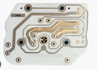
Manufacturing and Design Flexibility
Modern ceramic PCB manufacturing technologies have evolved to provide designers with increased flexibility and performance options.
Advanced Manufacturing Processes
Several specialized processes have been developed for ceramic PCB production:
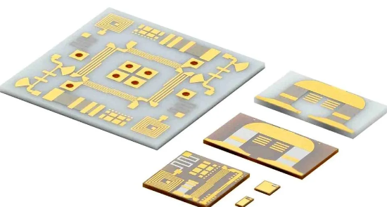
- Direct Bonded Copper (DBC):
- Copper foil bonded directly to ceramic substrate
- Excellent thermal conductivity and current-carrying capacity
- Widely used in power modules
- Direct Plated Copper (DPC):
- Thin-film deposition process for fine features
- Enables high-density interconnects
- Suitable for RF and microwave applications
- Low-Temperature Co-fired Ceramic (LTCC):
- Multi-layer structures co-fired at ~900°C
- Allows integration of passive components
- Used in RF modules and sensors
- High-Temperature Co-fired Ceramic (HTCC):
- Fired at 1300-1700°C
- Uses refractory metals (W, Mo, Mn)
- For extreme environment applications
Miniaturization Capabilities
Ceramic substrates support advanced miniaturization:
- Fine line/space resolution (down to 20μm)
- High-density interconnects
- Thin substrates (as low as 0.1mm)
- 3D packaging possibilities
These capabilities enable:
- Compact power modules
- Miniature sensors
- High-density RF components
- Advanced packaging solutions
Integration with Advanced Technologies
Ceramic substrates facilitate integration with:
- Embedded passive components (resistors, capacitors)
- Through-substrate vias (TSVs) for 3D integration
- Advanced thermal management solutions
- Hybrid packaging approaches
Diverse Industry Applications
The unique combination of properties offered by ceramic PCB substrates has led to their adoption across numerous industries and applications.
Automotive Electronics
Key applications include:
- Electric vehicle power electronics (inverters, converters)
- Battery management systems
- Engine control units
- LED lighting systems
- ADAS (Advanced Driver Assistance Systems)
The automotive industry particularly values ceramic substrates for:
- High-temperature operation under hood
- Vibration resistance
- Long-term reliability in harsh conditions
Aerospace and Defense
Critical applications in this sector:
- Avionics systems
- Radar and communication equipment
- Satellite electronics
- Missile guidance systems
- High-reliability military electronics
Ceramic substrates are preferred for their:
- Radiation resistance
- Extreme temperature performance
- Resistance to mechanical shock and vibration
Power Electronics
Widespread use in:
- IGBT modules
- Power converters and inverters
- Solid-state relays
- High-power RF amplifiers
- Renewable energy systems
Advantages for power applications:
- Efficient heat dissipation from high-power devices
- High voltage isolation
- Long-term reliability under thermal cycling
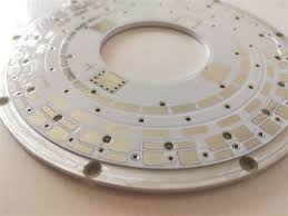
LED Lighting
Ceramic substrates are ideal for:
- High-power LED packages
- Automotive lighting
- Industrial and street lighting
- UV LED applications
Benefits include:
- Effective heat removal from LED junctions
- Long lifespan under continuous operation
- Stable performance at high temperatures
Medical Electronics
Important applications:
- Implantable devices (pacemakers, neurostimulators)
- Surgical instruments
- Diagnostic imaging equipment
- High-frequency ablation devices
Medical advantages:
- Biocompatibility (for certain ceramics)
- Sterilization resistance
- Long-term reliability in critical applications
Telecommunications
Growing use in:
- 5G base station components
- RF power amplifiers
- Microwave circuits
- Satellite communication equipment
Telecom benefits:
- Low signal loss at high frequencies
- Thermal stability for power amplifiers
- Miniaturization capabilities
Future Trends and Developments
The ceramic PCB substrate market continues to evolve with several emerging trends shaping its future.
Material Innovations
Ongoing developments include:
- Enhanced AlN formulations with improved thermal conductivity
- Novel ceramic composites with tailored properties
- Environmentally friendly alternatives to BeO
- Cost-reduction strategies for wider adoption
Manufacturing Advancements
Emerging production technologies:
- Additive manufacturing for complex geometries
- Improved multilayer fabrication techniques
- Higher precision patterning methods
- Automated production for cost reduction
Market Growth Drivers
Key factors propelling market expansion:
- Rapid growth in electric vehicles and charging infrastructure
- 5G network deployment and expansion
- Increasing adoption in renewable energy systems
- Growing demand for high-reliability electronics
Projections indicate significant market growth, with the Chinese ceramic substrate market alone expected to reach ¥7 billion (approximately $1 billion) by 2025.
Integration with Advanced Packaging
Future directions include:
- 2.5D and 3D integration with ceramic interposers
- Heterogeneous integration approaches
- System-in-Package (SiP) solutions
- Advanced thermal management architectures
Conclusion
Ceramic PCB substrates have established themselves as indispensable components in modern electronics, offering a unique combination of thermal, electrical, mechanical, and environmental properties that address the most challenging requirements of advanced electronic systems. From their exceptional thermal conductivity that enables efficient heat dissipation to their outstanding high-frequency performance and remarkable durability in harsh environments, ceramic substrates provide solutions that traditional organic materials cannot match.
As electronic systems continue to evolve toward higher power densities, greater miniaturization, and more demanding operating conditions, the importance of ceramic PCB substrates will only grow. Ongoing material innovations and manufacturing advancements promise to further enhance their performance while potentially reducing costs, enabling even broader adoption across industries.
Whether in the electric vehicles transforming transportation, the 5G networks enabling next-generation communications, or the advanced medical devices improving healthcare, ceramic PCB substrates are playing a critical role in powering technological progress. Their unique advantages ensure they will remain at the forefront of electronic materials technology, enabling the development of smaller, more powerful, and more reliable electronic systems for years to come.


