The Anatomy and Design of Graphics Card PCBs
Introduction
The graphics card, often referred to as the GPU (Graphics Processing Unit), is one of the most critical components in modern computing, especially for tasks requiring high-performance graphics rendering, such as gaming, 3D modeling, and machine learning. At the heart of every graphics card lies the Printed Circuit Board (PCB), a complex and meticulously designed substrate that connects and powers the various components of the GPU. This article delves into the intricacies of graphics card PCBs, exploring their design, components, and the challenges faced in their development.
1. The Role of the PCB in a Graphics Card
The PCB is the backbone of any graphics card, serving as the platform upon which all other components are mounted and interconnected. Its primary functions include:
- Electrical Connectivity: The PCB provides the electrical pathways that connect the GPU, memory, power delivery components, and other peripherals. These pathways, known as traces, are carefully designed to ensure efficient signal transmission and minimal interference.
- Mechanical Support: The PCB offers structural integrity to the graphics card, holding all components in place and ensuring they are securely connected.
- Thermal Management: Modern graphics cards generate significant heat, and the PCB plays a role in dissipating this heat. Copper layers within the PCB help conduct heat away from critical components, and the PCB design often includes provisions for mounting cooling solutions like heatsinks and fans.
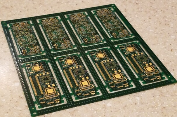
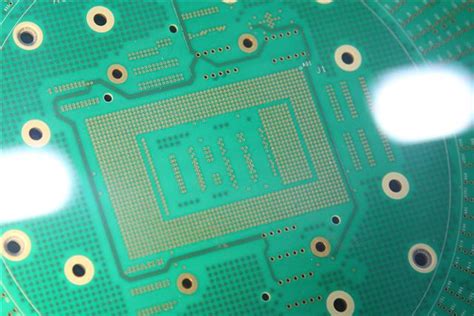
2. Layers and Materials
Graphics card PCBs are typically multi-layered, meaning they consist of several layers of conductive and insulating materials. The number of layers can vary depending on the complexity and performance requirements of the card, with high-end GPUs often featuring 10 or more layers.
- Conductive Layers: These are typically made of copper and form the traces that carry electrical signals between components. The thickness and width of these traces are carefully calculated to handle the required current and minimize resistance.
- Insulating Layers: These layers, usually made of fiberglass-reinforced epoxy (FR-4), separate the conductive layers and prevent electrical shorts. The choice of insulating material affects the PCB’s thermal and electrical properties.
- Solder Mask: This is a protective layer applied over the copper traces to prevent oxidation and short circuits. It also provides the PCB with its characteristic green (or sometimes black, red, or blue) color.
- Silkscreen: This layer is used for labeling components, indicating polarity, and providing other important information for assembly and troubleshooting.
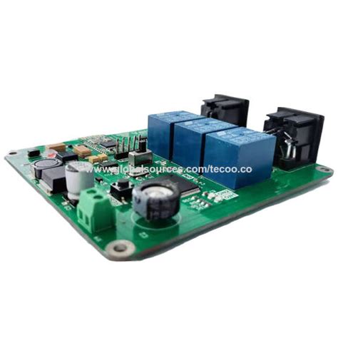
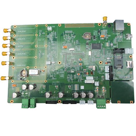
3. Key Components on the PCB
A graphics card PCB hosts a variety of components, each playing a crucial role in the card’s overall performance:
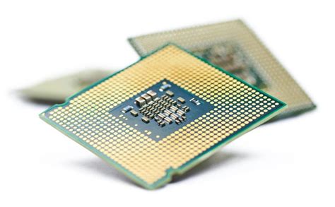
- GPU (Graphics Processing Unit): The GPU is the most critical component, responsible for rendering images, videos, and 3D graphics. It is usually the largest chip on the PCB and is often located near the center.
- VRAM (Video Random Access Memory): VRAM is specialized memory used to store textures, frame buffers, and other data required for rendering. It is typically located around the GPU and connected via high-speed traces.
- Power Delivery Components: These include voltage regulator modules (VRMs), capacitors, inductors, and MOSFETs. They ensure that the GPU and other components receive stable and clean power, which is essential for maintaining performance and longevity.
- PCIe Interface: The PCIe (Peripheral Component Interconnect Express) interface connects the graphics card to the motherboard. It provides both data transfer and power to the card.
- Display Outputs: These include HDMI, DisplayPort, and DVI connectors, which allow the graphics card to output video signals to monitors.
- Cooling Solutions: While not part of the PCB itself, the mounting points for heatsinks, fans, and other cooling solutions are integrated into the PCB design.
4. PCB Design Considerations
Designing a graphics card PCB is a complex process that involves balancing performance, power efficiency, thermal management, and manufacturability. Key considerations include:
- Signal Integrity: High-speed signals, such as those between the GPU and VRAM, must be carefully routed to minimize signal degradation and interference. This often involves using differential pairs, controlled impedance traces, and careful placement of components.
- Power Integrity: The power delivery network must be designed to provide stable voltage levels to the GPU and other components, even under heavy load. This involves careful placement of VRMs, capacitors, and other power components, as well as the use of multiple power and ground planes.
- Thermal Management: The PCB must be designed to efficiently dissipate heat, which involves the use of thermal vias, copper pours, and strategic placement of components to minimize hot spots.
- Manufacturability: The design must be feasible to manufacture at scale, which involves considerations such as component placement, trace routing, and the use of standard PCB fabrication processes.
5. Challenges in PCB Design
Designing a graphics card PCB presents several challenges, particularly as GPUs become more powerful and complex:
- Increasing Power Demands: Modern GPUs require significant amounts of power, which places greater demands on the power delivery network. This can lead to challenges in maintaining stable voltage levels and managing heat.
- Higher Clock Speeds: As GPU clock speeds increase, maintaining signal integrity becomes more challenging. High-speed signals are more susceptible to interference and signal degradation, requiring more sophisticated routing techniques.
- Thermal Management: With higher power consumption comes increased heat generation. Effective thermal management is critical to prevent overheating, which can lead to reduced performance or even hardware failure.
- Miniaturization: As consumers demand smaller and more compact graphics cards, PCB designers must find ways to fit more components into a smaller space without compromising performance or reliability.
6. Future Trends in Graphics Card PCB Design
The future of graphics card PCB design is likely to be shaped by several emerging trends:
- Advanced Materials: The use of advanced materials, such as high-performance laminates and thermally conductive substrates, could improve signal integrity and thermal management.
- 3D Packaging: Techniques such as 3D stacking of components could allow for more compact designs and improved performance by reducing the distance between components.
- AI and Machine Learning: AI-driven design tools could help optimize PCB layouts for signal integrity, power delivery, and thermal management, leading to more efficient and reliable designs.
- Integration with Other Technologies: As graphics cards are increasingly used in applications beyond gaming, such as AI and machine learning, PCB designs may need to incorporate additional features, such as specialized connectors or co-processors.
Conclusion
The PCB is a critical component of any graphics card, serving as the foundation upon which all other components are built. Its design involves a delicate balance of electrical, thermal, and mechanical considerations, and it must be carefully engineered to meet the demanding performance requirements of modern GPUs. As technology continues to advance, the design of graphics card PCBs will continue to evolve, incorporating new materials, techniques, and technologies to meet the ever-increasing demands of consumers and industries alike.