The Art of Handcrafting Printed Circuit Boards: A Step-by-Step Guide
Introduction
In an era dominated by automated PCB manufacturing and quick-turn prototyping services, the art of handcrafting printed circuit boards remains a valuable skill for electronics enthusiasts, students, and professionals alike. Manual PCB fabrication offers unparalleled flexibility for rapid prototyping, educational purposes, and low-volume production without the need for expensive equipment or external services. This comprehensive 2000-word guide will walk you through the complete process of creating professional-quality PCBs by hand, from design to final assembly.
1. Designing Your Circuit
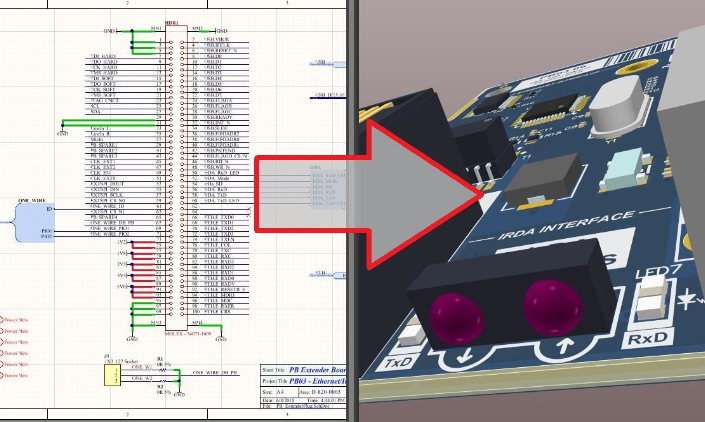
1.1 Schematic Creation
Before any physical work begins, proper circuit design is essential. Use EDA (Electronic Design Automation) software like:
- KiCad (open-source)
- Eagle (now Fusion 360)
- Altium Designer (professional)
- Fritzing (beginner-friendly)
Create a schematic that includes all components with proper values and connections. Verify your design through simulation if possible.
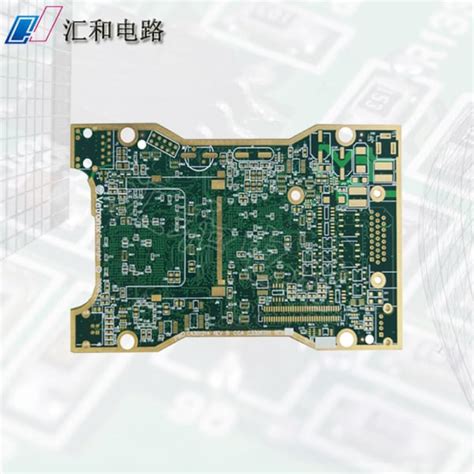
1.2 PCB Layout Design
Convert your schematic to a PCB layout, paying attention to:
- Component placement for optimal functionality
- Trace routing considering current requirements
- Proper clearance between traces (typically 0.3mm minimum)
- Drill hole sizes for components
- Board dimensions and mounting holes
1.3 Design Verification
Perform Design Rule Checks (DRC) to identify:
- Unconnected nets
- Short circuits
- Manufacturing rule violations
Generate Gerber files (even for manual fabrication) as they provide precise dimensional information.
2. Materials and Tools Preparation
2.1 Essential Materials
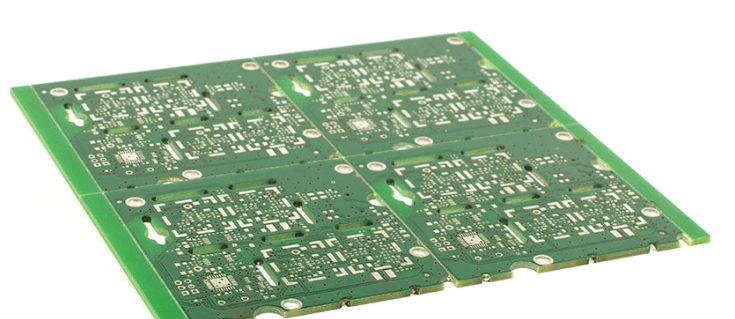
- Copper-clad board (FR-4 most common)
- Toner transfer paper or photo-sensitive board (depending on method)
- Ferric chloride or ammonium persulfate etchant
- Isopropyl alcohol (for cleaning)
- Fine-grit sandpaper (600-1000 grit)
- Permanent marker (for touch-ups)
- Drill bits (0.8mm-1.2mm for standard components)
- Solder mask (optional)
- Silkscreen materials (optional)
2.2 Required Tools
- Laser printer (for toner transfer method)
- Clothes iron or laminator (for transfer)
- Plastic or glass etching tray
- Drill press or rotary tool (Dremel)
- UV exposure unit (for photo-sensitive method)
- Precision knife set
- Metal ruler
- Tweezers
- Safety equipment (gloves, goggles, ventilation)
3. PCB Fabrication Process
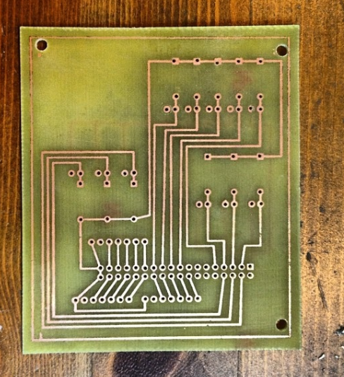
3.1 Board Preparation
- Cut the copper-clad board to size using a hacksaw or scoring tool
- Clean the copper surface with fine sandpaper to remove oxidation
- Wipe with isopropyl alcohol to eliminate grease and debris
3.2 Pattern Transfer Methods
Method A: Toner Transfer
- Print your PCB layout mirrored on glossy paper or special transfer paper using a laser printer
- Place the printed side against the copper surface
- Apply heat using a clothes iron (medium heat) or laminator (190°C)
- Apply even pressure for 5-10 minutes
- Soak the paper in warm water and gently rub to remove paper fibers
Method B: Photo-sensitive Resist
- Apply photo-sensitive film to clean copper or use pre-coated boards
- Print your design on transparent film (laser or inkjet)
- Expose the board to UV light through the film (exposure time varies)
- Develop the image using sodium hydroxide solution
3.3 Etching Process
- Prepare etchant solution (typically 1:3 ferric chloride to water)
- Place board in plastic tray and pour etchant over it
- Agitate gently to speed up the process (5-20 minutes depending on temperature)
- Remove when all unwanted copper is dissolved
- Rinse thoroughly with water
- Remove resist with acetone or sandpaper
3.4 Drilling Holes
- Mark drill locations using the original design as reference
- Use appropriate drill bits:
- 0.8mm for standard through-hole components
- 1.0mm for larger leads
- 1.2mm for connectors and mounting holes
- Secure the board firmly while drilling
- Drill perpendicular to the board surface to avoid angled holes
- Clean drill holes with a small drill bit or needle to remove burrs
3.5 Finishing Touches
- Inspect traces for breaks or shorts
- Repair minor flaws with conductive paint or wire bridges
- Apply solder mask (optional):
- UV-curable solder mask
- Liquid solder mask applied by brush
- Add silkscreen markings (optional)
- Apply surface finish (optional):
- Tin plating solution
- Conformal coating for protection
4. Component Assembly
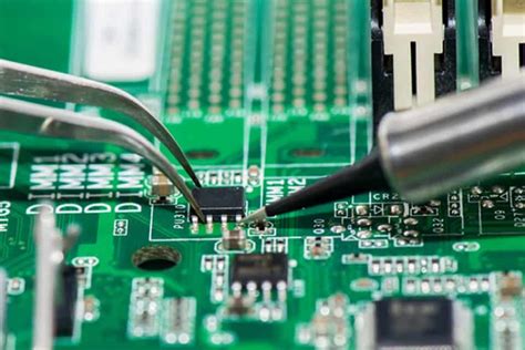
4.1 Soldering Techniques
- Start with the lowest profile components (resistors, diodes)
- Progress to taller components (capacitors, connectors)
- Use appropriate soldering iron temperature (300-350°C for leaded solder)
- Apply solder to the joint, not the iron tip
- Maintain 1-2 seconds contact time per joint
- Inspect for cold joints or bridges
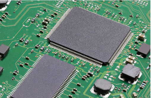
4.2 Special Components
- ICs: Use sockets for DIP packages or solder directly for SMD
- Heat-sensitive components: Work quickly or use heat sinks
- Surface-mount devices (SMD):
- Use tweezers for placement
- Apply solder paste or tack one pad first
- Drag solder technique for multi-pin components
5. Testing and Troubleshooting
5.1 Visual Inspection
- Check for proper solder joints (shiny, concave meniscus)
- Verify component orientation (diodes, electrolytic capacitors)
- Look for solder bridges or cold joints
5.2 Continuity Testing
- Use a multimeter to check:
- Power rail shorts to ground
- Proper connections between points
- Unintended connections (shorts)
5.3 Power-Up Testing
- Initial test without ICs installed
- Verify power supply voltages
- Check current draw for abnormalities
- Install ICs one by one, testing after each
5.4 Common Issues and Solutions
- Open circuits: Reflow solder or add jumper wires
- Short circuits: Use isopropyl alcohol to locate bridges
- Non-functioning sections: Verify component values and orientation
- Intermittent connections: Reflow suspicious joints
6. Advanced Techniques
6.1 Double-Sided Boards
- Align both sides using registration holes
- Use pins to maintain alignment during soldering
- Connect layers with through-hole plating or wire vias
6.2 Surface Mount Technology (SMT)
- Hand placement with fine-tip tweezers
- Stencil application of solder paste
- Hot air rework station for reflow
6.3 Professional Finishes
- Electroless nickel immersion gold (ENIG) plating
- HASL (Hot Air Solder Leveling)
- OSP (Organic Solderability Preservative)
7. Safety Considerations
- Always work in a well-ventilated area
- Use chemical-resistant gloves when handling etchants
- Wear eye protection during drilling and chemical processes
- Properly dispose of used chemicals (neutralize acids before disposal)
- Be cautious with hot tools (irons, soldering equipment)
- Keep a fire extinguisher rated for electrical fires nearby
8. Advantages and Limitations
Advantages:
- Immediate results without waiting for external fabrication
- Low cost for prototypes and small quantities
- Complete control over the entire process
- Educational value in understanding PCB manufacturing
- Ability to make quick design iterations
Limitations:
- Limited to relatively simple designs
- Lower precision than professional fabrication
- Time-consuming for complex boards
- Difficult to achieve fine pitch components (<0.5mm)
- Challenging for multi-layer boards
Conclusion
Mastering the art of handmade PCB fabrication provides electronics enthusiasts and professionals with a powerful skill that bridges the gap between concept and reality. While commercial PCB services offer higher precision for complex designs, the ability to quickly produce prototype boards by hand remains an invaluable capability in many situations. Through careful attention to each step—from design to etching to assembly—you can create professional-quality circuit boards that rival manufactured ones in functionality.
As you gain experience with manual PCB fabrication, you’ll develop your own techniques and refinements to the process. The satisfaction of holding a fully functional circuit board that you designed and fabricated entirely by yourself is unmatched, and the skills you develop will serve you throughout your electronics journey. Whether you’re a student learning the fundamentals, a hobbyist creating custom projects, or a professional needing rapid prototypes, handcrafted PCBs remain a relevant and rewarding aspect of electronics work.