The Art of PCB Design: Where Engineering Meets Aesthetics
Introduction to PCB Art
Printed Circuit Board (PCB) art represents a fascinating intersection of technology and creativity, where the functional requirements of electronics meet artistic expression. Traditionally viewed as purely utilitarian components hidden inside electronic devices, PCBs have emerged as a medium for artistic creation in their own right. This unique art form transforms the copper traces, solder masks, and component arrangements that make up circuit boards into visually striking designs that can be appreciated both for their technical function and aesthetic value.
PCB art has grown from a niche hobby among electrical engineers into a recognized art movement, with exhibitions, online communities, and even commercial applications. Artists and engineers alike are discovering that the constraints of PCB manufacturing can inspire rather than limit creativity, leading to works that are beautiful, functional, and sometimes both simultaneously.
The Origins and Evolution of PCB Art
The roots of PCB art can be traced back to the early days of circuit board manufacturing in the mid-20th century. While initially purely functional, some engineers began to recognize the aesthetic potential of the intricate copper traces they were designing. The first intentional PCB artworks likely emerged from engineers adding small personal touches to their designs—hidden messages, simple shapes, or signatures etched in copper.
As PCB manufacturing technology advanced, so did the possibilities for artistic expression. The introduction of colored solder masks in the 1980s opened new creative avenues, allowing artists to work with different background colors beyond the standard green. The development of more precise etching and drilling techniques enabled increasingly detailed designs.
The digital revolution of the 1990s and 2000s played a crucial role in PCB art’s development. Computer-aided design (CAD) software became more accessible and sophisticated, allowing designers to create complex patterns with relative ease. Online communities formed where enthusiasts could share their creations, techniques, and manufacturing tips, helping the art form to grow and evolve.
Today, PCB art exists on a spectrum from purely decorative pieces to fully functional circuits that also serve as artworks. Some artists create PCBs that serve no electronic purpose whatsoever, while others design circuits where the artistic elements are integral to the board’s function.
Technical Aspects of Creating PCB Art
Creating PCB art requires a unique combination of artistic vision and technical knowledge about circuit board design and manufacturing. Artists must work within the constraints of PCB production while finding creative ways to express their ideas within those limitations.
Design Software and Tools
Most PCB art begins in electronic design automation (EDA) software, the same tools used for conventional circuit board design. Popular programs include:
- KiCad (open-source)
- Eagle (now Fusion 360 Electronics)
- Altium Designer
- OrCAD
- DipTrace
These programs allow artists to create copper trace patterns, define solder mask areas, and place components. Some artists supplement these with vector graphics software like Adobe Illustrator or Inkscape to create more complex artwork that can then be imported into the PCB design tools.
Layers and Materials
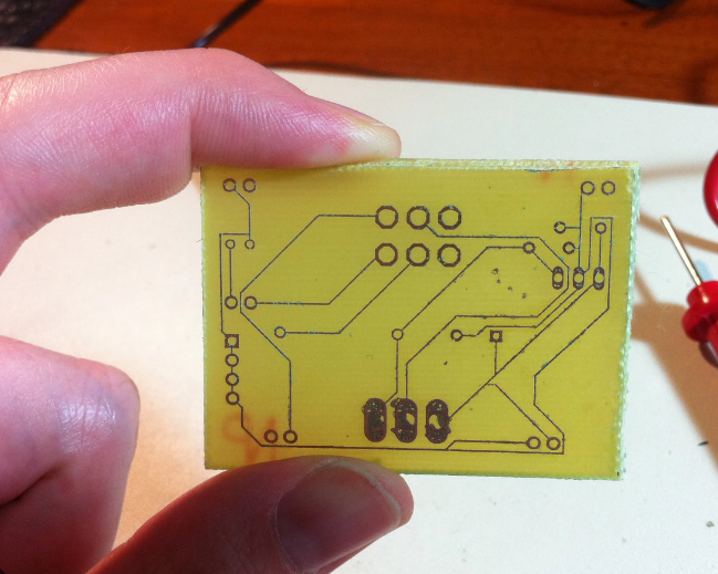
Understanding PCB layers is crucial for creating effective artwork. A typical PCB consists of:
- Copper layers: The conductive traces that can be shaped into artistic patterns
- Solder mask: The colored coating that covers most of the board, leaving only exposed copper where needed
- Silkscreen: The white (or other color) printing used for labels and markings
- Substrate: Usually FR-4 fiberglass, but other materials can be used for artistic effect
Artists manipulate these layers to create contrast and visual interest. For example, they might use the solder mask to create a colored background with copper traces forming the detailed artwork, or they might use the silkscreen layer to add fine details or text.
Manufacturing Considerations
PCB art must adhere to the same manufacturing constraints as functional circuit boards:
- Minimum trace width: Typically 0.1mm or larger depending on the manufacturer
- Clearance between traces: Usually 0.1mm or more to prevent short circuits
- Drill hole sizes: Mechanical drills have size limitations
- Board thickness: Standard is 1.6mm, but other options are available
Successful PCB artists learn to work within these limitations while still achieving their artistic vision. Some manufacturers specialize in artistic PCBs and may offer more flexible options than conventional PCB fabricators.
Styles and Techniques in PCB Art
PCB artists have developed numerous styles and techniques to create visually striking works. Some common approaches include:
Trace-based Art
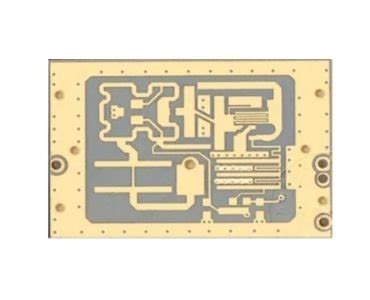
This style uses the copper traces themselves to create intricate patterns, often resembling line drawings or etchings. Artists carefully route circuit paths to form images, sometimes incorporating actual circuit functionality into the design. The traces might represent anything from portraits to landscapes to abstract patterns.
Solder Mask Art
By creatively using the solder mask layer, artists can create colored areas on the board. This might involve leaving large areas of copper exposed (which will oxidize to a distinctive patina over time) or using the solder mask to create color fields and shapes. Some manufacturers offer multiple solder mask colors on a single board, enabling more complex color designs.
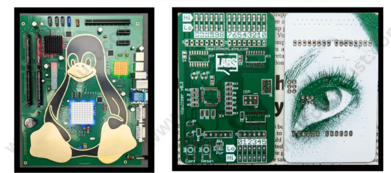
Component-based Art
In this approach, the electronic components themselves become part of the artwork. Resistors, capacitors, and ICs are arranged to form patterns or images when viewed from above. This technique often results in works that are both functional circuits and visual artworks.
Hybrid Art
Many PCB artworks combine multiple techniques, using traces, solder mask, silkscreen, and components together to create complex compositions. Some artists even incorporate non-traditional elements like LEDs that make the artwork interactive or dynamic.
Notable PCB Artists and Works
The PCB art community includes both professional engineers and dedicated artists. Some notable figures include:
- Saar Drimer – Known for his “Boldport” projects that combine beautiful PCB design with functional electronics
- Mohit Bhoite – Creates intricate PCB sculptures that often incorporate mechanical elements
- Jiri Praus – Produces stunning PCB-based jewelry and decorative items
- Eric Pan (Seeed Studio) – Has promoted PCB art through manufacturing services and exhibitions
Famous PCB artworks include:
- The “Twitter Machine” – A functional Twitter client with a bird-shaped PCB
- “The Kiss” by Boldport – A PCB interpretation of Gustav Klimt’s famous painting
- Various open-source hardware projects that incorporate artistic PCB designs
Functional vs. Decorative PCB Art
PCB art exists along a spectrum from purely decorative to fully functional:
Decorative PCB Art:
- Created solely for visual appeal
- May contain no actual circuitry
- Often used as wall art, jewelry, or decorative objects
- Allows complete artistic freedom in design
Functional PCB Art:
- Fully working electronic devices
- Artistic elements integrated with circuit functionality
- Examples include audio amplifiers with artistic layouts or decorative IoT devices
- Requires balancing aesthetic and technical requirements
Many artists enjoy the challenge of creating works that are both beautiful and functional, seeing this as the purest expression of PCB art.

The Cultural Significance of PCB Art
PCB art represents more than just an interesting niche in both the art and engineering worlds. It serves several important cultural functions:
- Demystifying Technology: By making circuit boards beautiful and approachable, PCB art helps bridge the gap between technology and the general public.
- Celebrating Engineering Beauty: It reveals the inherent aesthetic qualities in functional designs that might otherwise go unnoticed.
- Preserving Technical Heritage: Some PCB artworks incorporate retro electronics elements, serving as homage to technological history.
- Encouraging STEAM Education: The combination of Science, Technology, Engineering, Art, and Mathematics makes PCB art an excellent educational tool.
- Promoting Open Culture: Many PCB artists share their designs openly, contributing to the open-source hardware movement.
Creating Your Own PCB Art: A Beginner’s Guide
For those interested in trying PCB art, here are some basic steps to get started:
- Learn PCB Design Basics: Familiarize yourself with fundamental concepts like layers, traces, and components.
- Choose Software: Start with free tools like KiCad or EasyEDA.
- Begin Simple: Create basic shapes or patterns before attempting complex designs.
- Study Examples: Examine existing PCB artworks to understand techniques.
- Find a Manufacturer: Many online PCB services are art-friendly (OSH Park, PCBWay, JLCPCB).
- Experiment: Try different combinations of traces, masks, and components.
- Join Communities: Online forums and social media groups can provide feedback and inspiration.
The Future of PCB Art
As technology evolves, so too will PCB art. Emerging trends and possibilities include:
- Advanced Manufacturing: Higher precision and new materials will enable more detailed artworks.
- 3D PCB Printing: Could allow for sculptural PCB artworks with complex geometries.
- Interactive Art: Incorporating sensors and LEDs to create responsive pieces.
- Biodegradable Electronics: Environmentally friendly PCB art materials.
- Mainstream Recognition: More gallery exhibitions and institutional acceptance.
The growing maker movement and increasing interest in STEAM education suggest that PCB art will continue to flourish as both an artistic practice and educational tool.
Conclusion
PCB art represents a unique synthesis of technical skill and creative vision, transforming what was once considered merely functional into something beautiful and expressive. It challenges our perceptions of where art can be found and demonstrates that creativity can flourish even within the constraints of engineering specifications.
As our world becomes increasingly technological, art forms like PCB design help humanize our relationship with technology, revealing its aesthetic dimension and making it more accessible. Whether as functional artworks, decorative pieces, or educational tools, PCB art has established itself as a vibrant and growing field at the intersection of art and technology.
For engineers, it offers a creative outlet and new way to appreciate their craft. For artists, it provides a novel medium with unique properties and challenges. And for the public, it serves as a reminder that beauty and innovation often go hand in hand. As PCB technology continues to advance, so too will the possibilities for artistic expression within this fascinating medium.