The Basic Process Flow of PCBA Assembly
Introduction
Printed Circuit Board Assembly (PCBA) is a fundamental process in electronics manufacturing that involves mounting and soldering electronic components onto a printed circuit board (PCB). This complex, multi-stage process transforms bare PCBs into functional electronic assemblies that power everything from smartphones to industrial equipment. Understanding the basic PCBA assembly process flow is essential for electronics manufacturers, engineers, and anyone involved in product development. This article will explore the key stages of PCBA assembly, from initial preparation to final testing, providing a comprehensive overview of modern electronics manufacturing techniques.
1. Preparation and Material Inspection
The PCBA process begins long before components meet the board. Proper preparation ensures smooth production and high-quality results.
1.1 PCB Inspection
Before assembly, bare PCBs undergo rigorous inspection:
- Visual examination for scratches, dents, or discoloration
- Verification of hole sizes and pad dimensions
- Checking for proper solder mask application
- Testing of continuity and insulation resistance
1.2 Component Verification
All electronic components must be verified:
- Matching part numbers with the Bill of Materials (BOM)
- Checking component values and tolerances
- Verifying package types and footprints
- Inspecting for physical damage or oxidation
1.3 Solder Paste Inspection
For surface mount technology (SMT) processes:
- Solder paste composition verification
- Checking viscosity and metal content
- Ensuring proper storage conditions

2. Solder Paste Application
The first physical step in PCBA assembly is applying solder paste to the PCB.
2.1 Stencil Preparation
A laser-cut stainless steel stencil is created:
- Precise apertures match PCB pad layouts
- Stencil thickness determines paste volume
- Nano-coatings may be applied for better release
2.2 Printing Process
Solder paste is applied through the stencil:
- Automatic squeegees spread paste evenly
- Optimal pressure and speed settings are crucial
- 2D or 3D inspection systems verify paste deposition
2.3 Post-Printing Inspection
Automated Optical Inspection (AOI) checks:
- Paste volume and consistency
- Alignment with pads
- Bridges or smearing defects
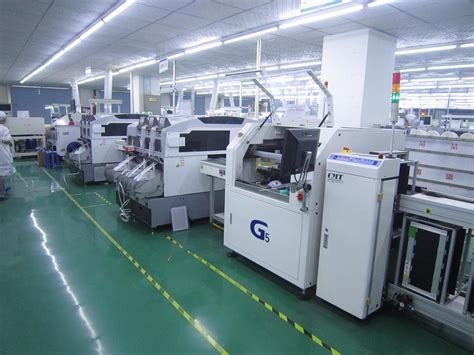
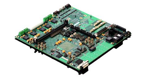
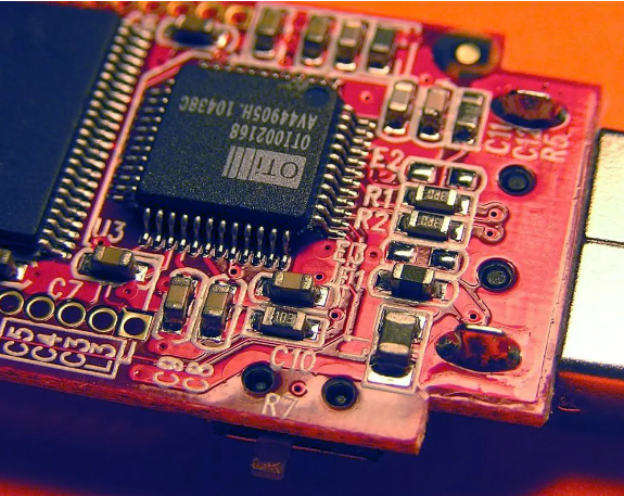
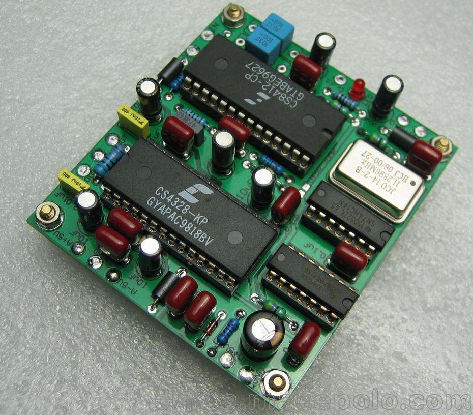
3. Surface Mount Technology (SMT) Component Placement
Modern PCBA relies heavily on automated SMT processes.
3.1 Pick-and-Place Machines
High-speed robotic systems place components:
- Vacuum nozzles pick components from reels or trays
- Vision systems ensure proper orientation
- Placement accuracy within ±25μm is typical
3.2 Component Types
SMT handles various packages:
- Passive components (resistors, capacitors)
- Integrated circuits (QFP, BGA, CSP)
- Connectors and electromechanical parts
3.3 Placement Verification
Post-placement inspection checks:
- Component presence and correct placement
- Polarity and orientation
- Tombstoning or shifting defects

4. Reflow Soldering
The solder paste must be melted to form permanent connections.
4.1 Reflow Oven Profile
A precisely controlled thermal process:
- Preheat zone gradually raises temperature
- Soak zone activates flux and equalizes temperatures
- Reflow zone melts solder (typically 220-250°C)
- Cooling zone solidifies joints
4.2 Atmosphere Control
Nitrogen may be used to:
- Reduce oxidation
- Improve wetting
- Enhance joint reliability
4.3 Post-Reflow Inspection
AOI systems examine:
- Solder joint quality
- Component position after reflow
- Bridges, voids, or insufficient solder
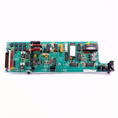
5. Through-Hole Technology (THT) Assembly
While SMT dominates, many assemblies still require through-hole components.
5.1 Component Insertion
Methods include:
- Manual insertion for prototypes or large components
- Automated insertion machines for high volume
- Mixed-technology boards may combine SMT and THT
5.2 Soldering Methods
Through-hole soldering options:
- Wave soldering: PCB passes over molten solder wave
- Selective soldering: Precise application to specific areas
- Hand soldering: For rework or delicate components
5.3 Post-Soldering Processes
Includes:
- Flux residue cleaning
- Lead trimming
- Visual inspection
6. Conformal Coating (Optional)
For boards operating in harsh environments.
6.1 Coating Types
Common materials include:
- Acrylic: Easy to apply and remove
- Silicone: High temperature resistance
- Urethane: Excellent moisture protection
- Parylene: Ultra-thin vapor deposition
6.2 Application Methods
Various techniques exist:
- Spray coating: Manual or automated
- Dipping: For complete coverage
- Selective coating: Precision application
6.3 Curing Process
Depending on material:
- Air drying
- UV curing
- Thermal curing
7. Testing and Quality Control
Final verification ensures functional boards.
7.1 In-Circuit Testing (ICT)
- Checks individual component values
- Verifies proper connections
- Tests basic functionality
7.2 Functional Testing
- Simulates actual operating conditions
- Verifies all features work properly
- May include burn-in testing
7.3 Automated Optical Inspection (AOI)
- High-resolution camera inspection
- Compares against known good boards
- Detects assembly defects
7.4 X-Ray Inspection
For hidden features:
- BGA solder joints
- Internal PCB layers
- Void detection
8. Final Assembly and Packaging
Preparing boards for shipment or integration.
8.1 Board Separation
For panelized PCBs:
- Depanelization via routing or scoring
- Careful handling to avoid stress
8.2 Cleaning
Removal of:
- Flux residues
- Handling contaminants
- Static charges
8.3 Packaging
Appropriate methods:
- Anti-static bags
- Protective foam
- Moisture barrier packaging
Conclusion
The PCBA assembly process represents a sophisticated integration of materials science, mechanical engineering, and quality control. From initial solder paste application to final functional testing, each stage builds upon the previous one to transform raw materials into complex electronic assemblies. As technology advances, PCBA processes continue to evolve with finer pitches, higher densities, and more automated inspection techniques. Understanding this fundamental process flow enables better design decisions, more efficient manufacturing, and higher quality electronic products. Whether producing consumer devices, industrial equipment, or aerospace components, mastery of PCBA assembly remains essential in our increasingly electronic world.