The Benefits of Eliminating Silkscreen on PCBs
Introduction
Printed Circuit Boards (PCBs) are essential components in modern electronics, providing the foundation for electrical connections between components. Traditionally, PCB designs include silkscreen—a layer of ink-printed text and symbols used for labeling components, test points, and other critical information. However, as PCB manufacturing technology advances, some designers are opting to eliminate silkscreen entirely. This article explores the benefits of omitting silkscreen from PCBs, including cost savings, improved manufacturing efficiency, enhanced signal integrity, and better aesthetics.
1. Cost Reduction
One of the most significant advantages of removing silkscreen from PCBs is cost savings. Silkscreen application involves additional materials, labor, and processing time, all of which contribute to higher production costs.
Lower Material Costs
Silkscreen requires specialized ink, stencils, and cleaning agents. Eliminating this step reduces material expenses, especially in high-volume production runs.
Reduced Manufacturing Steps
The silkscreen process involves printing, curing, and inspection. Removing it simplifies the manufacturing workflow, decreasing labor costs and potential delays.
Fewer Defects and Rework
Silkscreen misalignment, smudging, or fading can lead to rejected boards. Without silkscreen, manufacturers avoid these defects, improving yield rates and reducing rework expenses.
2. Improved Manufacturing Efficiency
Silkscreen application can slow down PCB production, particularly in complex designs. Omitting it streamlines the assembly process in several ways.
Faster Turnaround Time
Without silkscreen printing and curing, PCB fabrication becomes faster, enabling quicker delivery times—an advantage in rapid prototyping and just-in-time manufacturing.
Simplified Design Files
Designers no longer need to prepare silkscreen layers, reducing file complexity and potential errors in layer alignment.
Compatibility with Advanced PCB Technologies
High-density interconnect (HDI) PCBs and ultra-thin designs may not have sufficient space for silkscreen. Removing it allows for more compact and efficient layouts.
3. Enhanced Signal Integrity
In high-frequency and high-speed PCB designs, silkscreen can introduce unwanted effects that degrade performance.
Reduced Dielectric Interference
Silkscreen ink has a dielectric constant that can slightly alter impedance in sensitive RF and microwave circuits. Eliminating it ensures more consistent signal propagation.
Minimized Crosstalk
In tightly packed designs, silkscreen near high-speed traces can contribute to parasitic capacitance. Removing it helps maintain signal integrity.
Better Controlled Impedance
For impedance-controlled PCBs, even minor variations in dielectric properties matter. Without silkscreen, impedance calculations remain more accurate.
4. Better Aesthetics and Cleaner Designs
Modern electronics often prioritize sleek, minimalist designs. Silkscreen-free PCBs offer a cleaner, more professional appearance.
Smoother Surface Finish
Without silkscreen, the PCB surface is more uniform, improving the effectiveness of conformal coatings and solder masks.
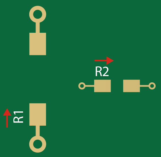
Improved Readability with Alternative Labeling
Instead of silkscreen, designers can use laser marking, engraved text, or QR codes for component identification—methods that are more durable and precise.
Enhanced High-Tech Appeal
Many premium electronics (e.g., smartphones, wearables) avoid silkscreen for a more polished look, reinforcing brand perception.
5. Increased Durability and Reliability
Silkscreen can wear off over time due to environmental exposure, handling, or cleaning processes. Removing it enhances long-term reliability.
No Fading or Peeling
Silkscreen degrades under heat, moisture, or chemical exposure. Without it, labels remain intact longer.
Better Resistance to Abrasion
In harsh environments, silkscreen can scratch off, making maintenance difficult. Alternative marking methods (e.g., laser etching) are more durable.
Improved Solderability
Incorrect silkscreen placement near pads can interfere with solder paste application. Its absence reduces soldering defects.
6. Flexibility in Miniaturization
As PCBs shrink, silkscreen becomes impractical. Advanced packaging techniques benefit from its removal.
More Space for Traces and Components
Eliminating silkscreen frees up space for additional routing or smaller component footprints.
Support for Advanced Assembly Techniques
Flip-chip, wafer-level packaging, and 3D-printed electronics often omit silkscreen to maximize functionality in limited areas.
7. Environmental Benefits
Reducing silkscreen usage aligns with sustainable manufacturing practices.
Less Chemical Waste
Silkscreen inks and solvents contribute to hazardous waste. Eliminating them reduces environmental impact.
Lower Energy Consumption
Curing silkscreen requires energy-intensive processes. Removing this step decreases the carbon footprint of PCB production.
Conclusion
While silkscreen has been a standard feature in PCBs for decades, its elimination offers numerous advantages, including cost savings, improved manufacturing efficiency, enhanced signal integrity, better aesthetics, and increased durability. As PCB technology evolves, designers are increasingly adopting silkscreen-free approaches to meet the demands of high-performance, miniaturized, and environmentally conscious electronics. By leveraging alternative labeling methods and optimizing board layouts, manufacturers can produce higher-quality PCBs without relying on traditional silkscreen techniques.
In summary, the trend toward silkscreen-free PCBs reflects the industry’s push for innovation, efficiency, and sustainability—making it a compelling choice for future electronic designs.