The bridge between PCB and semiconductor: the mystery and application of package substrate
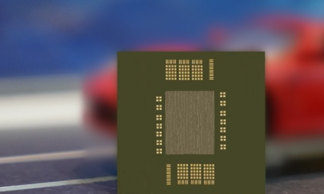
In the electronics industry, package substrate (Substrate, referred to as SUB) is an important component, which carries the chip and provides electrical connection, protection, support and heat dissipation for it. However, whether the package substrate belongs to PCB (printed circuit board) or semiconductor field is often a topic of discussion. This article will explore the relationship between package substrate, PCB and semiconductor from multiple perspectives such as the basic definition, function, manufacturing process and application field of package substrate, in order to provide readers with a clear understanding.
1.Basic definition and function of package substrate
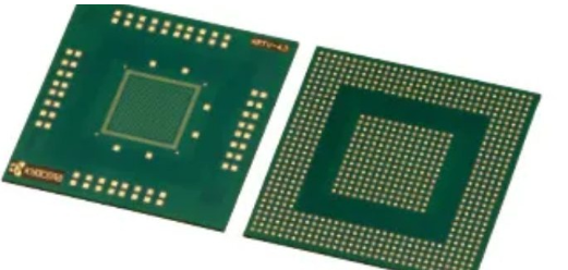
As the carrier of semiconductor chip, package substrate plays a vital role in the production process of integrated circuit chip. It is usually made of materials such as metal or ceramic, with good thermal conductivity, protection performance and mechanical strength. In the chip packaging process, the package substrate not only provides physical support and protection for the chip, but also realizes the electrical connection between the chip and the external circuit through its internal circuit structure.
Specifically, the package substrate has the following main functions:
Electrical connection: The circuit structure inside the package substrate provides a connection path for the chip to the external circuit to ensure that the chip can work normally.
Protection: The package substrate can protect the chip from the influence of the external environment, such as humidity, temperature, dust, etc., thereby extending the service life of the chip.
Support: The package substrate provides a stable physical support for the chip to ensure the stability and reliability of the chip during the packaging process.
Heat dissipation: Since the chip generates a lot of heat during operation, the package substrate effectively dissipates the heat through its internal heat dissipation structure to prevent the chip from being damaged due to overheating.
2.The relationship between package substrate and PCB
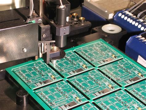
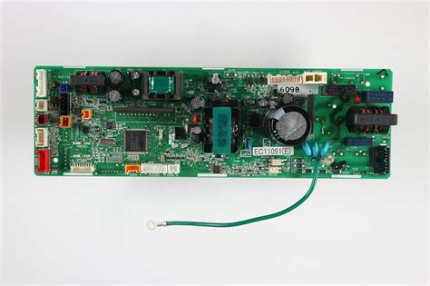
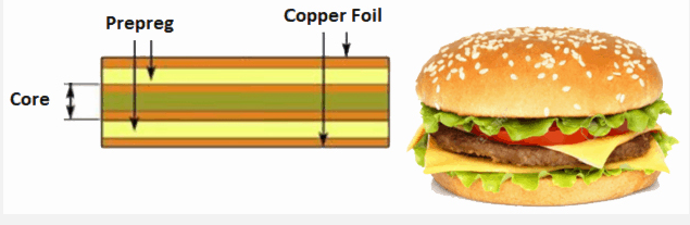
PCB (printed circuit board) is a printed circuit board used for connecting electronic components and transmitting signals. It is usually made of materials such as glass fiber and epoxy resin, and is processed through graphic design, photoresist coating, exposure and development, etching, deposition and other process flows. PCB is widely used in electronic devices, such as computers, mobile phones, tablets, etc., and is one of the key components to realize the functions of electronic devices.
Although package substrates and PCBs are both core components of circuit boards, they have significant differences in functions, manufacturing processes and application fields. Package substrates are mainly used in the manufacture of integrated circuit chips, playing the role of carrying and protecting chips; while PCBs are widely used in various electronic devices, with complex designs and high-precision processing technology.
Specifically, the main differences between packaging substrates and PCBs are reflected in the following aspects:
Function: The packaging substrate mainly serves chip packaging, providing support, heat dissipation, protection and electrical connection for the chip; while PCB is mainly used for the connection and signal transmission of electronic components.
Manufacturing process: The manufacturing process of the packaging substrate includes multiple processes such as cutting, polishing, and punching, which have extremely high requirements for precision and quality; while the manufacturing process of the PCB includes graphic design, photoresist coating, exposure and development, etching, deposition and other process flows.
Application field: The packaging substrate is mainly used in the field of integrated circuit chip manufacturing; while PCB is widely used in various electronic devices.
In addition, the packaging substrate can be regarded as a technical branch of PCB, which has the characteristics of high density, high precision, high performance, miniaturization and thinness. It provides electrical connection and physical support between the chip and the PCB motherboard, and is one of the core materials in the chip packaging link.
3.The relationship between packaging substrates and semiconductors
Semiconductors refer to materials whose electrical conductivity is between conductors and insulators at room temperature. Semiconductors are widely used in integrated circuits, consumer electronics, communication systems, photovoltaic power generation, lighting, high-power power conversion and other fields. For example, a diode is one of the devices made of semiconductors.
There is a close relationship between packaging substrates and semiconductors. First, the packaging substrate is the carrier of semiconductor chip packaging. It carries the chip and provides electrical connection, protection, support and heat dissipation for it. Secondly, the production and manufacturing technology of packaging substrates involves knowledge of multiple disciplines such as electronics, physics, and chemical engineering, and is inseparable from the development of semiconductor technology.
Specifically, the application of packaging substrates in the semiconductor field is mainly reflected in the following aspects:
Chip packaging: The packaging substrate is a key component in the chip packaging process. It carries the chip and realizes the electrical connection between the chip and the external circuit through its internal circuit structure.
High density: With the continuous development of semiconductor technology, packaging substrates are moving towards high density. For example, build-up multilayer board (BUM) is a new PCB product technology that can achieve high density of packaging substrates.
Multifunctionality: The packaging substrate can not only carry and protect the chip, but also bury passive and active devices to achieve certain system functions. This makes the application of packaging substrates in the semiconductor field more extensive and diverse.
4.Classification and application of packaging substrates
Packaging substrates can be classified according to different classification standards. For example, according to different substrate materials, packaging substrates can be divided into inorganic packaging substrates and organic packaging substrates. Inorganic packaging substrates mainly include ceramic-based packaging substrates and glass-based packaging substrates; organic packaging substrates mainly include phenolic packaging substrates, polyester packaging substrates and epoxy resin packaging substrates.
In addition, packaging substrates can also be classified according to different application fields. For example, according to different application fields, packaging substrates can be divided into memory chip packaging substrates, logic chip packaging substrates, sensor chip packaging substrates and communication chip packaging substrates. These different types of packaging substrates play an important role in their respective application fields.
In terms of application, packaging substrates are widely used in various electronic devices, such as computers, mobile phones, tablets, etc. At the same time, with the continuous development of semiconductor technology, packaging substrates are also increasingly widely used in emerging fields such as high-performance computing, the Internet of Things, and artificial intelligence. For example, in the field of high-performance computing, packaging substrates can carry high-performance computing chips to achieve high-speed data processing and transmission; in the field of the Internet of Things, packaging substrates can carry components such as sensor chips to achieve the intelligence and interconnection of equipment.
5.Development Trends and Challenges of the Packaging Substrate Industry
The packaging substrate industry is characterized by high processing difficulty and investment threshold. From the perspective of product layers, board thickness, line width and line spacing, minimum ring width and other dimensions, packaging substrates tend to be more precise and miniaturized. This requires the use of high-precision and high-reliability technologies and equipment in the manufacturing process of packaging substrates. At the same time, with the continuous development of semiconductor technology, the packaging substrate industry is also facing higher and higher technical requirements and challenges.
However, the packaging substrate industry is also facing some challenges. First, the market competition in the packaging substrate industry is becoming increasingly fierce, and major manufacturers have increased their R&D investment and technological innovation efforts to improve the competitiveness and market share of their products. Secondly, with the increasingly obvious trend of miniaturization and lightweight of electronic equipment, packaging substrates also need to continuously reduce their size, reduce their weight and improve their performance to meet market demand. Finally, the packaging substrate industry also needs to pay attention to issues such as environmental protection and sustainable development, and use environmentally friendly materials and processes to reduce the impact on the environment.
In order to meet these challenges and opportunities, the packaging substrate industry needs to continue to innovate and develop. On the one hand, it is necessary to increase R&D investment and technological innovation to improve the precision, reliability and performance of products; on the other hand, it is necessary to strengthen cooperation and coordinated development with upstream and downstream industrial chains to form a complete industrial chain and ecological system. At the same time, it is also necessary to pay attention to market demand and trend changes and adjust product structure and market strategy in time to adapt to market changes and development.

6. Conclusion
In summary, packaging substrates are neither pure PCB fields nor completely equivalent to semiconductor fields. It is an interdisciplinary technology product between PCB and semiconductors, and plays an important role in integrated circuit chip manufacturing and electronic equipment. By deeply understanding the basic definition, function, manufacturing process, application field and industry development trend of packaging substrates, we can better grasp the status and role of packaging substrates in the electronics industry and provide strong support and guarantee for the development of related industries.