The charm of PCB design for RF and digital-analog circuits
How to design RF and digital-analog circuits on the same PCB?
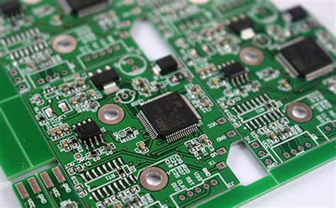
The proliferation of handheld wireless communications devices and remote control devices is driving significant growth in demand for hybrid analog, digital and RF designs. Handheld devices, base stations, remote controls, Bluetooth devices, computer wireless communications capabilities, numerous consumer appliances, and military/aerospace systems now require RF technology.
For several years, RF design has required professional designers to use specialized design and analysis tools.
Typically, the RF portion of the PCB is designed by RF professionals in a stand-alone environment and then merged with the rest of the mixed-technology PCB. This process is inefficient and often requires iterative design and multiple unrelated databases to integrate with hybrid technologies.
In the past, design functionality was performed and duplicated in two design environments and connected through a non-intelligent ASCII interface (Figure 1(a)). The PCB system design and RF specialized design systems in both environments have their own libraries, RF design databases and design archives. This requires that design data (schematics and layouts) and libraries in the two environments be managed and synchronized through a cumbersome ASCII interface.

Under this old approach, RF designers developed RF circuits in isolation from other parts of the PCB system design. The RF circuit is then translated into the overall PCB design using the ASCII file, creating the schematic and physical implementation on the main PCB. If there is a problem with the RF circuit, the design must be corrected in a separate RF solution and then re-translated into the main PCB.
The RF simulator only simulates ideal radio frequency circuits. There are many fragmented ground planes, ground planes, and adjacent RF circuits in actual hybrid system implementations, which makes analysis very difficult, and it is known that these additional shapes will have a long-term impact on the operation of the RF circuit.
This old approach has been successfully used for mixed-signal circuit board design for many years, but as the content of RF circuitry in products increases, the problems caused by two independent design systems have begun to affect designer productivity, time to market and product quality. quality.
To address these issues, Mentor Graphics has developed a dynamic link technology that integrates PCB schematic and layout tools with RF design and simulation tools, resulting in a new solution that overcomes traditional Disadvantages of RF design.
RF aware PCB design
To maintain design intent between PCB and RF design, the RF design tool must understand the layer-oriented structure of the PCB layout, and the PCB system must understand the parametric planar microwave components used in the RF design environment.
Another key issue is that the PCB system layouts the RF circuit as a short circuit, which prevents proper design rule verification (DRC) of the design. For today’s complex RF system designs, functional RF-aware DRC is a design methodology necessary to ensure correct design.
All of these help maintain design intent. Maintaining design intent is critical because it is the basis for enabling multiple round trips of design data between toolsets without losing information.
RF design is an iterative process, requiring many steps to adjust and optimize the design. In the past, RF design was very difficult in the context of a real PCB design. When an optimized RF module is implemented on a PCB, there is no guarantee that it will still work optimally. As a verification, electromagnetic field analysis (EM) of the PCB implementation is required.
There are several problems with this design process. First, the circuit is simulated as a simple metal layer geometry, so the RF tool cannot modify the metal layer and send the optimized results back to the PCB design and still have a good RF circuit. Secondly, EM solutions are time-consuming.
In the new flow, because the PCB tools and RF tools have a common understanding of the design intent, circuits can be moved between tool sets without losing the design intent. This means that circuit simulations (very quickly) and EM analyzes (when needed) can be performed repeatedly, and the results of each circuit modification can be compared. All this is done in a real PCB environment, including the ground plane, RF circuit layout, wires, vias and other components.
RF PCB design bottleneck
RF PCB design bottlenecks mainly include the following. First, since each RF module on the PCB board may have been designed by an independent RF design team, and each module can be independently upgraded, evolved, and reused, it becomes difficult to manage the entire circuit as a whole. It is crucial that these modules are still accessed as separate circuit elements at all times. To solve this problem, schematic and layout tools must be extended to support hierarchical grouped circuits. With this approach, even if an RF circuit is already laid out on the PCB, it can still be placed as an RF circuit with other modules and connected to the appropriate RF design team for analysis.
The next hurdle is designing the ground plane. In the traditional design process, RF metal is used as a black box metal block, and the distance from the ground is done manually because the air must pass through each stratum. When the RF circuit is updated (which is a frequent operation), the cut-out parts must be manually modified to correspond to the new circuit. For some designs, this editing process alone can take weeks.
New integrated design process
The integration between RF design tools and PCB design tools has always been based on the bidirectional conversion of ASCII IFF format files. Although this format can handle some design data, it is far from achieving seamless iterative synthesis. Lack of library synchronization is a fatal cause.
This design need resulted in a web-based tool-to-tool communication that provides a dynamic bidirectional link between RF design and system-level PCB design (Figure 1(b)). To support concurrent engineering processing, multiple PCB engineers can use the same design database simultaneously, each able to link one or more analog parts. Now, RF design tools can be used to design RF modules and, when appropriate, be synthesized as part of system-level schematics and PCBs, rather than being just an elusive black box circuit as in the past. At this stage, the circuit can be upgraded and its effects simulated in either environment.
Treat each RF circuit as a set of objects to help maintain traceability, version management and design issues. Because the design intent is preserved, any number of design iterations can be performed without time cost. In addition, because the RF module can be simulated in a real system-level PCB environment, its functionality should be verified in more detail to help shorten the design cycle.
Minimize RF effects in PCB interconnection design
The interconnection of the circuit board system includes: chip to circuit board, PCB intra-board interconnection, and three types of interconnection between PCB and external devices. In RF design, the electromagnetic characteristics at interconnection points are one of the main issues faced by engineering design. This article introduces various techniques for the above three types of interconnection design, including device installation methods, wiring isolation, and measures to reduce lead inductance. etc.
There are currently signs that printed circuit board designs are becoming more and more frequent.
As data rates continue to grow, the bandwidth required for data transmission has also pushed the upper limit of signal frequency to 1GHz or even higher. Although this high-frequency signal technology is far beyond the scope of millimeter wave technology (30GHz), it does also involve RF and low-end microwave technology.
RF engineering design methods must be able to handle the stronger electromagnetic field effects typically produced at higher frequency bands. These electromagnetic fields can induce signals on adjacent signal lines or PCB traces, causing unwanted crosstalk (interference and total noise) and damaging system performance. Return loss is primarily caused by impedance mismatch, which affects the signal in the same way as additive noise and interference.
High return loss has two negative effects:
1. The signal reflected back to the signal source will increase the system noise, making it more difficult for the receiver to distinguish the noise from the signal;
2. Any reflected signal will basically reduce the signal quality because the input signal The shape has changed.
Although the digital system only processes 1 and 0 signals and has very good fault tolerance, the harmonics generated when the high-speed pulse rises will cause the higher the frequency, the weaker the signal.
Although forward error correction technology can eliminate some negative effects, part of the system’s bandwidth is used to transmit redundant data, resulting in a reduction in system performance. A better solution is to have RF effects help rather than detract from signal integrity. It is recommended that the total return loss at the highest frequency of a digital system (usually the poorer data point) is -25dB, which is equivalent to a VSWR of 1.1.
The goals of PCB design are smaller, faster and lower cost
. For RFPCB, high-speed signals sometimes limit the miniaturization of PCB design. Currently, the primary approaches to solving crosstalk issues are ground plane management, spacing between traces, and reducing lead inductance (studcapacitance). The main method to reduce return loss is impedance matching. This approach includes effective management of insulation materials and isolation of active signal lines and ground lines, especially between signal lines that undergo state transitions and ground.
Since the interconnection point is the weakest link in the circuit chain, in RF design, the electromagnetic properties at the interconnection point are the main issues faced by the engineering design. It is necessary to examine each interconnection point and solve the existing problems. The interconnection of the circuit board system includes three types of interconnection: chip to circuit board, PCB intra-board interconnection, and signal input/output between PCB and external devices.
1.Interconnection between chip and PCB board
The Pentium IV and high-speed chips containing a large number of input/output interconnect points were already available. As for the chip itself, its performance is reliable and its processing rate can already reach 1GHz. One of the most exciting things to see at the recent GHz Interconnect Symposium (www.az.ww.com) is that the methods for dealing with the increasing number and frequency of I/Os are already well understood. The main problem with chip-PCB interconnection is that the interconnection density is too high, which causes the basic structure of the PCB material to become a factor limiting the growth of interconnection density. An innovative solution presented at the meeting was to use a local wireless transmitter inside the chip to transmit data to an adjacent circuit board.
Whether this solution is effective or not, the participants are very clear: in terms of high-frequency applications, IC design technology is far ahead of PCB design technology.
2.PCB intra-board interconnection
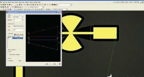
The techniques and methods for high-frequency PCB design are as follows:
- The corners of the transmission line should be at a 45° angle to reduce return loss (Figure 1);
- Use high-performance insulating circuit boards with insulation constant values strictly controlled by level. This approach facilitates effective management of electromagnetic fields between the insulating material and adjacent wiring.
- It is necessary to improve PCB design specifications for high-precision etching. Consider specifying a total line width tolerance of +/-0.0007 inches, managing the undercut and cross-section of the wiring shape, and specifying wiring sidewall plating conditions. Overall management of wiring (wire) geometry and coating surfaces is important to address skin effect issues associated with microwave frequencies and to achieve these specifications.
- There is a tap inductance in the protruding leads, so avoid using components with leads. In high frequency environments, it is best to use surface mount components.
- For signal vias, avoid using the via processing (pth) process on sensitive boards, because this process will cause lead inductance at the vias. For example, when a via on a 20-layer board is used to connect layers 1 to 3, the lead inductance can affect layers 4 to 19.
- Provide a rich ground layer. Molded holes should be used to connect these ground planes to prevent the impact of 3D electromagnetic fields on the circuit board.
- Choose electroless nickel plating or immersion gold plating process instead of HASL method for electroplating. This electroplated surface provides better skin effect for high-frequency currents (Figure 2). In addition, this highly solderable coating requires fewer leads, helping to reduce environmental pollution.
- The solder mask prevents the flow of solder paste. However, covering the entire board surface with solder mask will result in large changes in electromagnetic energy in microstrip designs due to thickness uncertainty and unknown insulation properties. Generally, a solder dam is used as the solder mask.
If you are unfamiliar with these methods, consult an experienced design engineer who has designed military microwave circuit boards. You can also discuss with them the price range you can afford. For example, it is more economical to use a copper-backedcoplanar microstrip design than a stripline design. You can discuss this with them to get better advice. Good engineers may not be used to thinking about cost issues, but their advice can be quite helpful. Now we must try our best to train young engineers who are unfamiliar with RF effects and lack experience in dealing with RF effects. This will be a long-term task.
In addition, other solutions can also be adopted, such as improving computer models to have the ability to handle RF effects.
3.Interconnection between PCB and external devices
Now it can be considered that we have solved all the signal management problems on the board and on the interconnection of various discrete components. So how to solve the problem of signal input/output from the circuit board to the wires connecting the remote devices? Trompeter Electronics, an innovator in coaxial cable technology, is working to solve this problem and has made some important progress (Figure 3). Also, take a look at the electromagnetic field given in Figure 4. In this case, we manage the conversion between microstrips and coaxial cables. In coaxial cable, the ground planes are interwoven in a ring and evenly spaced. In microstrip, the ground plane is below the active lines. This introduces certain edge effects that need to be understood, anticipated, and accounted for during design. Of course, this mismatch also results in return loss, which must be minimized to avoid noise and signal interference.
Managing impedance issues within a circuit board is not a design issue that can be ignored. The impedance starts at the surface of the circuit board, goes through a solder joint to the connector, and ends at the coaxial cable. Since impedance changes with frequency, impedance management becomes more difficult at higher frequencies. The problem of using higher frequencies to transmit signals over broadband appears to be a major design issue.


