The Comprehensive Guide to Graphics Card PCB Design and Architecture
Introduction to Graphics Card PCB
The printed circuit board (PCB) is the foundational component of any modern graphics card, serving as the central nervous system that connects and powers all other elements. As GPU technology has advanced from simple 2D accelerators to today’s massively parallel processing units capable of real-time ray tracing and AI acceleration, the complexity of graphics card PCBs has grown exponentially.
A graphics card PCB is far more than just a platform for mounting components—it’s a carefully engineered system that must balance electrical performance, thermal management, mechanical stability, and signal integrity while operating at increasingly high frequencies and power levels. Modern high-end graphics cards like the NVIDIA RTX 4090 or AMD RX 7900 XTX feature PCBs with 12-16 layers, sophisticated power delivery systems, and advanced cooling solutions to handle 300-600W of power dissipation.
This article will explore all aspects of graphics card PCB design, from basic layout principles to advanced manufacturing techniques, providing readers with a comprehensive understanding of this critical component in computer graphics hardware.
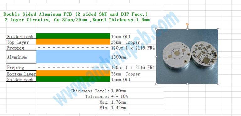
PCB Layers and Stackup
Layer Composition
Modern graphics card PCBs typically employ multilayer designs ranging from 6 layers in entry-level cards to 16 layers in flagship models. This layered approach allows for:
- Signal Layers: Dedicated to high-speed data transmission between components
- Power Planes: Distribute stable voltage to all components
- Ground Planes: Provide reference planes and reduce electromagnetic interference
A typical 10-layer graphics card PCB might use the following stackup:
- Top Layer (Component mounting and high-speed signals)
- Ground Plane
- Signal Layer
- Power Plane (1.8V/3.3V)
- Signal Layer
- Core Ground Plane
- Signal Layer
- Power Plane (12V)
- Signal Layer
- Bottom Layer (Component mounting and power delivery)
Material Selection
Most graphics cards use FR-4 (Flame Retardant 4) glass-reinforced epoxy laminate as the base material, with high-end models sometimes incorporating more advanced materials like:
- Isola FR408HR: For improved high-frequency performance
- Rogers RO4000: For critical RF sections
- Panasonic Megtron 6: For extreme high-speed designs
The dielectric constant (Dk) and dissipation factor (Df) of these materials become increasingly important as signal speeds exceed 10Gbps in modern interfaces like PCIe 4.0/5.0.
Power Delivery System
Voltage Regulation Modules (VRM)
The power delivery system on a graphics card PCB is responsible for converting the 12V input from the PCIe slot and power connectors to the various voltages required by different components:
- GPU Core: Typically 0.8V-1.2V at very high current (up to 500A peak)
- Memory: GDDR6/GDDR6X requires 1.35V-1.4V
- PLLs and I/O: Various voltages between 1.8V-3.3V
Modern graphics cards use multiphase buck converters with:
- PWM Controller: Modern digital controllers like Infineon XDPE132G5D or Monolithic Power Systems MP2888A
- Power Stages: High-current MOSFETs arranged in parallel phases (up to 24 phases on flagship cards)
- Chokes: High-efficiency alloy or ferrite core inductors
- Capacitors: A mix of polymer, tantalum, and ceramic capacitors for filtering
Power Connectors
The evolution of power connectors on graphics card PCBs has progressed from:
- Molex (Legacy)
- 6-pin PCIe (75W)
- 8-pin PCIe (150W)
- 12VHPWR (600W): Introduced with PCIe 5.0, featuring 16 pins and sideband signals
Proper power connector placement and PCB trace routing is critical to avoid voltage drops and ensure stable operation under load.
Signal Integrity Considerations
High-Speed Routing
Modern GPUs interface with memory and other components at extremely high frequencies:
- GDDR6/GDDR6X Memory: 14-24Gbps per lane
- PCIe 4.0/5.0: 16GT/s-32GT/s
- DisplayPort 2.1: Up to 80Gbps (UHBR20)
To maintain signal integrity at these speeds, PCB designers must:
- Match Trace Lengths: Keep differential pairs within 5-10 mils of each other
- Control Impedance: Typically 85-100Ω for differential pairs
- Minimize Vias: Each via introduces impedance discontinuity
- Proper Grounding: Provide uninterrupted return paths
Electromagnetic Interference (EMI) Mitigation
Techniques to reduce EMI in graphics card PCBs include:
- Shielding Cans: Over sensitive analog components
- Spread Spectrum Clocking: Reduces peak emissions
- Proper Layer Stacking: Alternating signal and ground/power layers
- Edge Plating: Often used along the PCIe connector edge
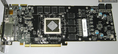
Component Placement and Layout
GPU Placement
The graphics processor is typically positioned:
- Centrally on the PCB for balanced trace routing
- With direct access to memory chips via short traces
- Aligned with the cooling solution’s vapor chamber or heat pipes
Memory Configuration
Modern graphics cards use memory chips (typically GDDR6/GDDR6X) arranged around the GPU in a configuration that:
- Minimizes trace lengths (usually <15mm)
- Provides equal access time from GPU to each memory chip
- Allows for proper power delivery to each memory IC
Common memory bus widths include:
- 128-bit (Entry-level)
- 192-bit (Mid-range)
- 256-bit (High-end)
- 384-bit (Flagship)
Additional Components
Other critical components on the PCB include:
- Display Outputs: DisplayPort, HDMI connectors
- Video BIOS Chip: Stores firmware and settings
- Fan Headers: For cooling system control
- RGB Lighting Controllers: For aesthetic elements
- Temperature Sensors: For thermal monitoring
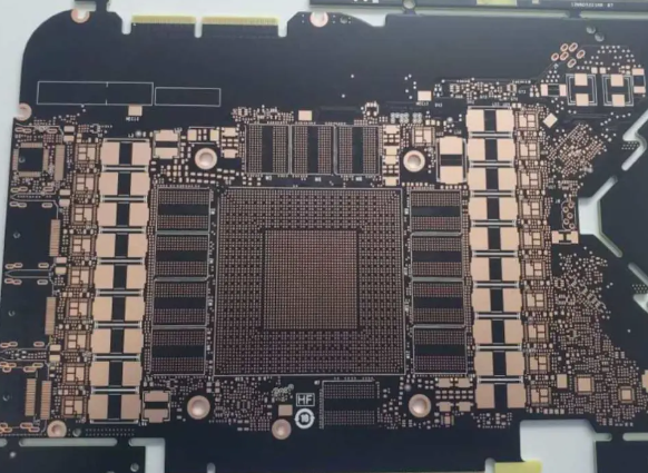
Manufacturing and Assembly
PCB Fabrication Process
The manufacturing of graphics card PCBs involves:
- Inner Layer Processing: Copper patterning and etching
- Lamination: Bonding layers under heat and pressure
- Drilling: For vias and component holes (laser drilling for microvias)
- Plating: Electroless and electrolytic copper deposition
- Solder Mask Application: Typically green or black
- Surface Finish: ENIG (Electroless Nickel Immersion Gold) or HASL (Hot Air Solder Leveling)
Component Assembly
Modern graphics cards use:
- SMT (Surface Mount Technology): For most components
- Reflow Soldering: For attaching SMT parts
- Selective Soldering: For through-hole components
- Underfill Application: For large BGA components like the GPU
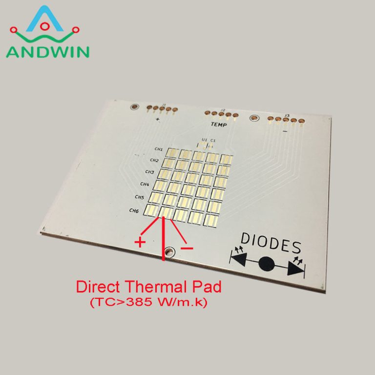
Thermal Management Integration
The PCB design must accommodate thermal solutions through:
- Thermal Pad Placement: For VRM and memory cooling
- Mounting Holes: For heatsink attachment
- Heat Spreader Integration: Some high-end cards use metal plates
- Thermal Via Arrays: Under high-power components
Reliability and Testing
Graphics card PCBs undergo rigorous testing including:
- Automated Optical Inspection (AOI): For assembly defects
- In-Circuit Testing (ICT): Verifies component functionality
- Burn-in Testing: Stress testing under load
- Signal Integrity Testing: Using VNAs and oscilloscopes
Future Trends in Graphics Card PCB Design
Emerging technologies influencing PCB design include:
- 3D Packaging: Such as NVIDIA’s CoWoS (Chip on Wafer on Substrate)
- Substrate-Like PCBs (SLP): For higher density interconnects
- Liquid Cooling Integration: Direct-to-chip cooling solutions
- Advanced Materials: For higher thermal conductivity
- Higher Layer Counts: To accommodate increasing complexity
Conclusion
The graphics card PCB represents one of the most sophisticated mass-produced circuit boards in consumer electronics, combining advanced materials science, electrical engineering, and thermal management into a single platform. As GPU technology continues to advance with higher performance targets and more specialized processing units, the underlying PCB designs will need to evolve accordingly—embracing new materials, manufacturing techniques, and architectural approaches to meet these challenges.
Understanding the complexities of graphics card PCB design provides valuable insight not just into computer hardware engineering, but into the broader field of high-speed digital design where signal integrity, power delivery, and thermal considerations must all be balanced to achieve optimal performance.