The Comprehensive Guide to PCB Board Production
Printed Circuit Boards (PCBs) are the backbone of modern electronics. They are used in almost every electronic device, from smartphones and computers to industrial machinery and medical equipment. The production of PCBs is a complex process that involves multiple steps, each requiring precision and expertise. This article provides a comprehensive guide to PCB board production, covering everything from design to final testing.
1. Introduction to PCBs
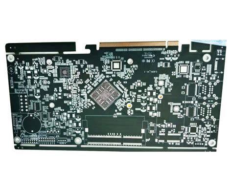
A Printed Circuit Board (PCB) is a flat board made of insulating material, such as fiberglass, with conductive pathways etched or printed onto its surface. These pathways, known as traces, connect various electronic components, such as resistors, capacitors, and integrated circuits, to form a functional electronic circuit.
PCBs come in various types, including single-sided, double-sided, and multi-layer boards. Single-sided PCBs have conductive traces on one side only, while double-sided PCBs have traces on both sides. Multi-layer PCBs consist of multiple layers of conductive traces separated by insulating layers, allowing for more complex circuits.
2. PCB Design
The first step in PCB production is the design phase. This involves creating a schematic diagram of the circuit, which is then converted into a physical layout using specialized software. The layout defines the placement of components and the routing of traces.
2.1 Schematic Design
The schematic design is a graphical representation of the circuit, showing how components are connected. It is created using Electronic Design Automation (EDA) software, such as Altium Designer, Eagle, or KiCad. The schematic includes symbols for each component and lines representing the electrical connections between them.
2.2 PCB Layout
Once the schematic is complete, the next step is to create the PCB layout. This involves placing the components on the board and routing the traces that connect them. The layout must consider factors such as signal integrity, power distribution, and thermal management.
The layout is typically created using the same EDA software used for the schematic. The software provides tools for component placement, trace routing, and design rule checking (DRC) to ensure that the design meets manufacturing requirements.
2.3 Design Rule Checking (DRC)
Design Rule Checking (DRC) is a critical step in the PCB design process. It involves verifying that the design adheres to the manufacturing rules and constraints, such as minimum trace width, spacing between traces, and hole sizes. DRC helps to prevent manufacturing defects and ensures that the PCB can be produced reliably.
3. PCB Fabrication
Once the design is finalized, the next step is PCB fabrication. This involves converting the digital design into a physical board. The fabrication process consists of several steps, each of which is described below.
3.1 Material Selection
The first step in PCB fabrication is selecting the appropriate materials. The most common base material for PCBs is FR-4, a type of fiberglass-reinforced epoxy laminate. Other materials, such as polyimide or ceramic, may be used for specialized applications.
The conductive layers are typically made of copper, which is laminated onto the base material. The thickness of the copper layer is specified in ounces per square foot, with 1 oz/ft² being the most common.
3.2 Printing the Circuit Pattern
The next step is to transfer the circuit pattern from the digital design onto the copper-clad board. This is done using a process called photolithography.
3.2.1 Photoresist Application
A layer of photoresist is applied to the copper surface. Photoresist is a light-sensitive material that hardens when exposed to ultraviolet (UV) light.
3.2.2 Exposure
The PCB layout is printed onto a transparent film, known as a photomask. The photomask is placed over the photoresist-coated board, and the assembly is exposed to UV light. The areas of the photoresist exposed to light harden, while the unexposed areas remain soft.
3.2.3 Development
After exposure, the board is developed by washing it with a chemical solution. This removes the unexposed photoresist, leaving behind a pattern of hardened photoresist that matches the circuit design.
3.3 Etching
The next step is to remove the unwanted copper from the board, leaving only the traces defined by the photoresist pattern. This is done using a chemical etching process.
The board is immersed in an etching solution, typically ferric chloride or ammonium persulfate, which dissolves the exposed copper. The hardened photoresist protects the copper traces, preventing them from being etched away.
3.4 Stripping
After etching, the remaining photoresist is stripped away using a chemical solution, revealing the copper traces. The board is then cleaned to remove any residual chemicals.
3.5 Drilling
Holes are drilled into the board to accommodate through-hole components and vias (connections between layers). The drilling process is typically done using computer-controlled drilling machines, which ensure precise hole placement.
3.6 Plating
The drilled holes are plated with copper to create electrical connections between layers. This is done using an electroplating process, where the board is immersed in a copper sulfate solution and an electric current is applied. The copper ions in the solution are deposited onto the walls of the holes, forming a conductive layer.
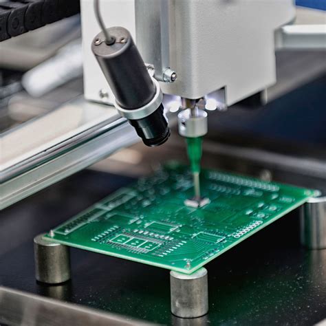
3.7 Solder Mask Application
A solder mask is applied to the board to protect the copper traces from oxidation and prevent solder bridges during assembly. The solder mask is typically a green epoxy layer that is applied using a screen printing process.
The solder mask is then cured using UV light, and any excess material is removed.
3.8 Silkscreen Printing
The final step in the fabrication process is silkscreen printing. This involves adding text, labels, and component identifiers to the board using a special ink. The silkscreen layer helps with component placement during assembly and provides information for troubleshooting and repair.
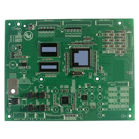
4. PCB Assembly
Once the PCB is fabricated, the next step is assembly. This involves mounting and soldering the electronic components onto the board.
4.1 Component Placement
The components are placed onto the board according to the design layout. This can be done manually for small-scale production or using automated pick-and-place machines for large-scale production.
4.2 Soldering
The components are soldered onto the board to create electrical connections. There are two main soldering methods used in PCB assembly: wave soldering and reflow soldering.
4.2.1 Wave Soldering
Wave soldering is used for through-hole components. The board is passed over a wave of molten solder, which flows into the holes and creates connections between the component leads and the copper traces.
4.2.2 Reflow Soldering
Reflow soldering is used for surface-mount components. Solder paste, a mixture of solder particles and flux, is applied to the board using a stencil. The components are then placed onto the solder paste, and the board is heated in a reflow oven. The solder paste melts, creating electrical connections between the components and the board.
4.3 Inspection and Testing
After assembly, the PCB is inspected and tested to ensure that it functions correctly. This may include visual inspection, automated optical inspection (AOI), and electrical testing.
4.3.1 Visual Inspection
Visual inspection involves checking the board for defects such as solder bridges, misaligned components, and missing parts. This can be done manually or using automated systems.
4.3.2 Automated Optical Inspection (AOI)
AOI uses cameras and image processing software to detect defects in the solder joints and component placement. AOI systems can quickly and accurately identify issues that may be missed during manual inspection.
4.3.3 Electrical Testing
Electrical testing involves verifying that the PCB functions as intended. This may include continuity testing, where the electrical connections are checked for opens and shorts, and functional testing, where the board is powered up and its performance is evaluated.
5. Final Finishing and Packaging
Once the PCB has passed inspection and testing, it undergoes final finishing and packaging. This may include applying a conformal coating to protect the board from environmental factors, such as moisture and dust, and packaging the board for shipment.
5.1 Conformal Coating
Conformal coating is a protective layer applied to the PCB to protect it from environmental factors. The coating is typically a thin layer of acrylic, silicone, or urethane that is applied using a spray, brush, or dip process.
5.2 Packaging
The final step is packaging the PCB for shipment. The boards are typically placed in anti-static bags to prevent damage from electrostatic discharge (ESD) and packed in boxes with protective padding to prevent damage during transit.
6. Conclusion
PCB production is a complex and multi-step process that requires precision and expertise. From the initial design phase to final testing and packaging, each step plays a critical role in ensuring that the final product meets the required specifications and functions correctly.
Advances in technology have led to the development of more sophisticated PCB manufacturing techniques, allowing for the production of increasingly complex and high-performance boards. As the demand for smaller, faster, and more reliable electronic devices continues to grow, the importance of PCB production will only continue to increase.
Whether you are a designer, engineer, or manufacturer, understanding the PCB production process is essential for creating high-quality electronic products. By following the steps outlined in this guide, you can ensure that your PCBs are produced to the highest standards, meeting the needs of today’s demanding electronic applications.


