The Comprehensive Guide to PCB Buried Vias: Design, Manufacturing, and Applications
1. Introduction to PCB Buried Vias
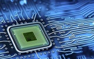
Printed Circuit Boards (PCBs) are the backbone of modern electronics, enabling the interconnection of various components in compact and efficient layouts. As electronic devices become more complex and miniaturized, PCB designers must adopt advanced techniques to accommodate higher component densities. One such technique is the use of buried vias, which play a crucial role in high-density interconnect (HDI) PCBs.
This article explores buried vias, their advantages, manufacturing processes, design considerations, and applications in modern electronics.
2. What Are Buried Vias?
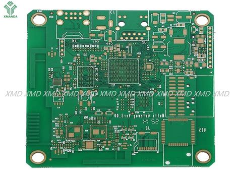
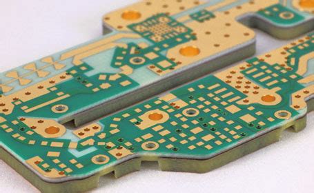
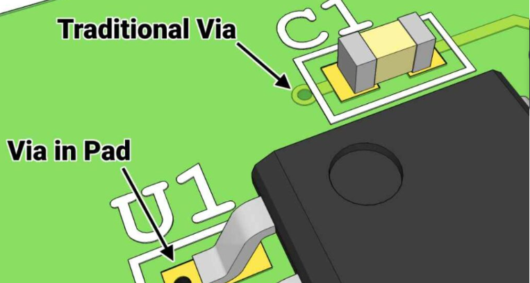
A buried via is a type of interconnect structure in a multilayer PCB that connects inner layers without reaching the outer surfaces of the board. Unlike through-hole vias (which span the entire board) or blind vias (which connect an outer layer to an inner layer), buried vias are entirely internal and invisible from the outside.
Key Characteristics of Buried Vias:
- Located between inner layers of a PCB.
- Not visible on the top or bottom surfaces.
- Used to increase routing density without consuming surface space.
- Essential for HDI (High-Density Interconnect) PCBs.
3. Advantages of Using Buried Vias
Buried vias offer several benefits in advanced PCB designs:
3.1 Space Efficiency
- By avoiding surface connections, buried vias free up space for additional components and routing channels.
- Ideal for miniaturized devices like smartphones, wearables, and IoT modules.
3.2 Improved Signal Integrity
- Reduces stub effects (unused via portions that can cause signal reflections).
- Minimizes crosstalk and electromagnetic interference (EMI) by optimizing signal paths.
3.3 Enhanced Reliability
- Since buried vias are protected within the PCB, they are less prone to mechanical damage or environmental exposure.
- Reduces the risk of solder joint failures compared to surface vias.
3.4 Support for Complex Multilayer Designs
- Enables higher layer counts (e.g., 8+ layers) without excessive via congestion.
- Facilitates high-speed digital and RF designs by optimizing layer transitions.
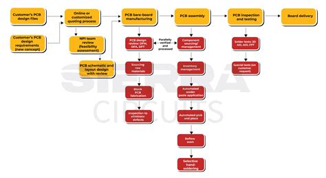
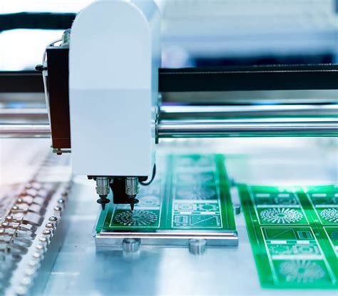
4. Manufacturing Process of Buried Vias
The production of buried vias involves precise laser drilling and sequential lamination processes. Below is a step-by-step overview:
4.1 Layer Preparation
- Inner layers are fabricated separately with copper traces and pads.
- Laser or mechanical drilling creates microvias in the required layers.
4.2 Via Formation
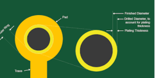
- Laser Drilling: A high-precision laser creates small-diameter holes (typically 50-150 µm).
- Plating: The holes are electroplated with copper to establish conductivity.
4.3 Lamination and Bonding
- Multiple inner layers with buried vias are stacked and laminated under high pressure and temperature.
- Additional layers are added, and the process repeats for complex multilayer PCBs.
4.4 Final PCB Assembly
- After lamination, the PCB undergoes outer layer patterning, soldermask application, and surface finishing.
Challenges in Manufacturing Buried Vias:
✔ Higher cost due to additional lamination steps.
✔ Tighter tolerances require advanced equipment.
✔ Inspection difficulties (since vias are hidden, X-ray or cross-sectioning may be needed).
5. Design Considerations for Buried Vias
To maximize the benefits of buried vias, PCB designers must follow best practices:
5.1 Via Size and Aspect Ratio
- Smaller vias (e.g., 0.1mm diameter) allow higher density but require precise plating.
- Aspect ratio (depth/diameter) should be ≤ 1:1 for laser-drilled vias to ensure proper copper deposition.
5.2 Layer Stackup Planning
- Optimize layer assignments to minimize unnecessary via transitions.
- Avoid placing buried vias in high-stress areas (e.g., near bends or connectors).
5.3 Signal and Power Integrity
- Use buried vias for critical signal paths to reduce EMI.
- Ensure proper return paths for high-speed signals.
5.4 Thermal Management
- Buried vias can help dissipate heat but must avoid creating thermal bottlenecks.
6. Applications of Buried Vias in Modern Electronics
Buried vias are widely used in advanced PCB designs, including:
6.1 Consumer Electronics
✔ Smartphones & Tablets – Enables thinner, more compact designs.
✔ Wearable Devices – Supports flexible and rigid-flex PCBs.
6.2 High-Performance Computing
✔ Servers & GPUs – Enhances signal integrity in high-speed data transfer.
✔ AI/ML Hardware – Facilitates complex multilayer interconnects.
6.3 Automotive & Aerospace
✔ ADAS (Advanced Driver Assistance Systems) – Ensures reliability in harsh environments.
✔ Satellite Communication PCBs – Reduces weight while maintaining performance.
6.4 Medical Devices
✔ Implantable Electronics – Provides robust, space-efficient interconnects.
✔ Diagnostic Equipment – Supports high-frequency signal integrity.
7. Comparison with Other Via Types
| Feature | Buried Via | Blind Via | Through-Hole Via |
|---|---|---|---|
| Visibility | Internal | One side | Both sides |
| Cost | High | Medium | Low |
| Complexity | High | Medium | Low |
| Use Case | HDI PCBs | Mid-density | Standard PCBs |
8. Future Trends in Buried Via Technology
- 3D Printed Electronics: Additive manufacturing may simplify buried via fabrication.
- Advanced Materials: Low-loss dielectrics improve high-frequency performance.
- AI-Driven PCB Design: Machine learning optimizes via placement for signal integrity.
9. Conclusion
Buried vias are a critical technology in modern PCB design, enabling higher density, better performance, and enhanced reliability. While they add complexity and cost, their benefits in HDI, high-speed, and miniaturized applications make them indispensable.
As electronics continue to evolve, buried vias will play an even greater role in next-generation devices, from 5G infrastructure to advanced medical implants. Designers and manufacturers must continue refining buried via techniques to meet the demands of future technologies.