The Comprehensive Guide to PCB Solder Mask: Materials, Processes, and Applications
Introduction to PCB Solder Mask
Printed Circuit Board (PCB) solder mask, also known as solder resist or solder stop mask, is a critical protective layer applied to the copper traces of a PCB. This thin lacquer-like polymer coating serves multiple essential functions in modern electronics manufacturing, making it indispensable for reliable circuit board production.
The primary purpose of solder mask is to prevent solder bridges from forming between closely spaced solder pads during the assembly process. By covering the areas where solder isn’t required, it ensures proper electrical isolation and prevents short circuits. Beyond this fundamental role, solder mask also provides environmental protection for copper traces against oxidation, moisture, and contamination while offering mechanical protection against scratches and abrasion during handling and use.
Historically, PCBs in the early days of electronics often lacked solder mask entirely. As circuit densities increased and component sizes shrank throughout the 1960s and 1970s, the need for this protective layer became apparent. Today, solder mask is considered standard for nearly all PCB designs except the most basic prototypes.
Modern solder masks have evolved into sophisticated materials that contribute to both the functionality and aesthetics of circuit boards. They’re available in various colors (with green being the most traditional and common), and can even include special formulations for high-frequency applications or extreme environments. The development of solder mask technology has paralleled the advancement of PCB manufacturing as a whole, with each new generation of electronics demanding more from this crucial protective layer.
Types of Solder Mask Materials
The electronics industry employs several types of solder mask materials, each with distinct properties and suitable applications. The most common variants include:
Liquid Photoimageable Solder Mask (LPSM): This is currently the most widely used solder mask in PCB manufacturing. LPSM is applied as a liquid coating and then cured through a photolithographic process. It offers excellent resolution for fine-pitch components and comes in two main formulations:
- Liquid Epoxy-based: Known for good chemical resistance and mechanical properties
- Liquid Acrylic-based: Offers faster curing times and good flexibility
Dry Film Solder Mask (DFSM): Applied as a solid film laminated onto the PCB surface, DFSM provides uniform thickness and is particularly suitable for boards with very flat surfaces. While it offers excellent coverage, it’s less capable of conforming to highly uneven surfaces compared to liquid masks. DFSM typically shows superior chemical resistance and is often used in high-reliability applications.
Topside and Bottom-side Solder Masks: These refer to masks applied to specific sides of the PCB rather than different material types. The same material is typically used on both sides, though some designs might call for different properties on each side.
Specialty Solder Masks:
- Flexible solder masks: Designed for use with flex and rigid-flex PCBs, these formulations can withstand repeated bending without cracking
- High-temperature solder masks: Formulated to endure the extreme temperatures encountered in certain manufacturing processes or operating environments
- UV-curable solder masks: Cure quickly under UV light, offering manufacturing efficiency advantages
- Low-Dk solder masks: Optimized for high-frequency applications where dielectric constant is critical
The choice between these materials depends on multiple factors including the PCB’s intended application, manufacturing process requirements, environmental conditions, and cost considerations. LPSM remains the most popular for general applications due to its good balance of performance, resolution, and cost-effectiveness.
Solder Mask Application Process
The application of solder mask is a multi-step process that requires precision and careful control to ensure optimal results. While exact methods may vary between manufacturers and specific solder mask types, the general process follows these key stages:
1. Surface Preparation:
Before applying solder mask, the PCB surface must be thoroughly cleaned and prepared. This typically involves:
- Mechanical brushing or chemical cleaning to remove oxides and contaminants
- Micro-etching to roughen the copper surface slightly for better adhesion
- Rinsing and drying to ensure no residues remain
2. Solder Mask Application:
The method of application varies by solder mask type:
- Liquid Photoimageable Solder Masks are typically applied using:
- Curtain coating (for high-volume production)
- Spray coating (for complex boards with uneven surfaces)
- Screen printing (for simpler designs or low-volume runs)
- Dry Film Solder Masks are laminated onto the board using heat and pressure
3. Pre-drying (for liquid masks):
The coated boards undergo a pre-drying (or “tack drying”) stage to evaporate solvents and create a semi-cured surface ready for imaging. This is typically done in convection ovens at controlled temperatures.
4. Imaging and Exposure:
The solder mask is then exposed to UV light through a photomask (also called a solder mask artwork film):
- The photomask contains the negative image of where solder mask should remain
- Areas exposed to UV light polymerize and become insoluble
- Unexposed areas remain soluble and will be removed in development
5. Development:
The board is processed through a developer solution (usually alkaline) that removes the unexposed, uncured solder mask, revealing the underlying copper pads and features that need to be solderable.
6. Final Curing:
The solder mask undergoes complete polymerization through:
- Thermal curing (for thermally cured materials)
- Additional UV exposure (for UV-curable materials)
- Combination processes (for dual-cure materials)
7. Inspection and Quality Control:
The finished solder mask undergoes rigorous inspection, which may include:
- Visual inspection under magnification
- Automated optical inspection (AOI)
- Thickness measurements
- Adhesion tests
- Solderability tests on exposed pads
Modern PCB factories often employ sophisticated equipment like laser direct imaging (LDI) systems that can expose the solder mask without physical photomasks, increasing accuracy and enabling finer feature resolution. The entire process is carefully controlled with parameters like coating thickness, exposure energy, development time, and curing profiles all optimized for the specific solder mask material and PCB design requirements.
Color Options and Their Significance
While traditional PCBs are most commonly associated with green solder mask, modern manufacturing offers a spectrum of color options, each with its own practical and aesthetic considerations:
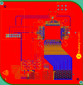
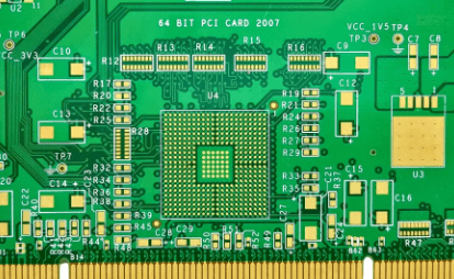
Green: The most traditional and widely used solder mask color. Green offers excellent contrast with white silkscreen, making identification of components and markings easy. It provides good visibility for automated optical inspection (AOI) systems and has proven reliability over decades of use.
Red: Offers high contrast with copper traces, making it popular for demonstration boards or educational purposes where trace visibility is desired. Red solder masks typically have similar performance characteristics to green.
Blue: Becoming increasingly popular, especially for consumer electronics where aesthetics matter. Blue provides good contrast with white markings and is often associated with high-quality boards.
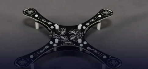
Black: Provides a sleek, professional appearance but can make inspection more challenging due to low contrast with traces. Black masks may absorb more heat during soldering processes and can show scratches or imperfections more visibly.
White: Primarily used for LED boards where light reflection is important. White solder masks can yellow over time when exposed to heat or UV light and may show contamination more readily.
Yellow: Offers excellent contrast with black silkscreen markings but can make automated optical inspection slightly more challenging compared to green.
Clear/Transparent: Used when copper trace visibility is essential, such as in some debugging or educational scenarios. Provides minimal protection against UV light.
The choice of solder mask color can impact the manufacturing process in several ways:
- Different pigments may affect the curing characteristics of the mask
- Some colors may require slightly different exposure times during imaging
- Darker colors (especially black) can make laser marking of serial numbers more challenging
- Certain colors may affect the thermal properties during soldering processes
While color selection often comes down to aesthetic preference or corporate branding, it’s important to note that not all colors are created equal in terms of performance. Green remains the most reliable and thoroughly tested option, with other colors potentially showing variations in:
- Adhesion to copper and substrate materials
- Resistance to chemicals and solvents
- Thermal stability during soldering processes
- Long-term durability under UV exposure
For high-reliability applications or extreme environments, it’s often advisable to stick with traditional green unless specific requirements justify an alternative color choice. Manufacturers can provide data sheets showing performance characteristics for their various color options to help designers make informed decisions.
Technical Specifications and Performance Characteristics
Solder mask performance is defined by several key technical specifications that determine its suitability for different applications and environments. Understanding these parameters is essential for PCB designers and manufacturers:
1. Resolution and Registration Accuracy:
- Minimum feature size (typically 50-75μm for LPSM)
- Alignment accuracy relative to copper features (±25-50μm standard)
- Ability to define small openings for fine-pitch components
2. Thickness:
- Typical range: 15-25μm over copper, 25-50μm over substrate
- Must be thick enough for protection but not so thick as to cause soldering issues
- Thinner masks allow for finer feature definition
3. Dielectric Properties:
- Dielectric constant (Dk): Typically 3.5-4.5 at 1MHz
- Dissipation factor (Df): 0.02-0.04 at 1MHz
- Important for high-frequency applications where signal integrity is critical
4. Thermal Characteristics:
- Glass transition temperature (Tg): 120-150°C for standard masks
- Decomposition temperature: Typically >300°C
- Resistance to multiple soldering cycles (wave, reflow, hand soldering)
5. Mechanical Properties:
- Pencil hardness: Typically 6H-8H
- Flexibility (for flex circuit applications)
- Adhesion strength to copper and substrate (usually >5N/cm)
6. Chemical Resistance:
- Resistance to fluxes, solvents, cleaning agents
- Alkali resistance for development process compatibility
- Acid resistance for subsequent processing steps
7. Environmental Durability:
- UV stability (resistance to yellowing or degradation)
- Moisture absorption (typically <2%)
- Resistance to fungal growth (important for certain environments)
8. Solderability Performance:
- Non-wettability to prevent solder adhesion in masked areas
- Clean release from pads during soldering
- Resistance to solder ball formation
9. Electrical Properties:
- Insulation resistance: >10^8 megohms
- Dielectric strength: >50kV/mm
- Surface resistivity: >10^12 ohms/square
10. Safety and Compliance:
- UL recognition (typically 94V-0 flame rating)
- RoHS compliance (free of restricted substances)
- Halogen-free options available
These specifications vary between different solder mask formulations and manufacturers. High-reliability applications (military, aerospace, medical) often require solder masks with enhanced thermal and chemical resistance properties, while consumer electronics might prioritize cost-effectiveness and aesthetic qualities.
Modern solder mask technologies continue to evolve, with newer formulations offering:
- Improved thermal conductivity for better heat dissipation
- Lower dielectric constants for high-speed digital applications
- Enhanced flexibility for rigid-flex designs
- Better environmental friendliness with reduced VOC content
When selecting a solder mask, designers must balance these various characteristics against their specific application requirements, considering factors such as operating environment, expected lifespan, manufacturing processes, and end-use conditions.
Common Defects and Quality Control
Solder mask application, while a mature process, can still be prone to various defects that affect PCB quality and reliability. Understanding these potential issues and their causes is essential for effective quality control:
1. Solder Mask Misregistration:
- Misalignment between solder mask openings and underlying copper pads
- Causes: Improper artwork alignment, exposure tool inaccuracies, or dimensional instability of materials
- Effects: Can lead to exposed traces or partially covered pads, risking shorts or poor solderability
2. Solder Mask Slivering:
- Thin, fragile strands of solder mask bridging between features
- Typically occurs with very fine pitch designs
- Causes: Overexposure, improper development, or insufficient mask relief in design
3. Solder Mask Voids/Pinholes:
- Small uncovered spots in the mask layer
- Causes: Contamination during application, bubbles in liquid mask, or incomplete coating
- Effects: Potential for corrosion or unintended solder bridging
4. Solder Mask Peeling/Delamination:
- Separation of the mask from the PCB surface
- Causes: Poor surface preparation, contamination, or inadequate curing
- Effects: Exposes underlying copper to environmental damage and may lead to further peeling
5. Incomplete Cure:
- Solder mask remains partially uncured
- Causes: Insufficient UV exposure, incorrect curing temperature, or expired material
- Effects: Reduced chemical resistance and potential for mask degradation
6. Solder Mask Bleeding:
- Mask material flows onto areas meant to remain uncovered
- Causes: Excessive mask thickness, improper pre-drying, or overdevelopment
- Effects: Can reduce solderable area or cause component placement issues
7. Orange Peel Texture:
- Uneven surface finish resembling orange peel
- Causes: Improper spray coating parameters or viscosity issues with liquid mask
- Effects: Primarily cosmetic but may affect solder paste application
8. Solder Mask Discoloration:
- Unintended color changes, often yellowing
- Causes: Overcuring, contamination, or UV degradation
- Effects: Mostly cosmetic but may indicate material degradation
Quality Control Measures:
To prevent these defects and ensure consistent solder mask quality, manufacturers implement various QC processes:
- Visual Inspection: Manual examination under magnification (often 10x) for obvious defects
- Automated Optical Inspection (AOI): Camera-based systems compare the actual mask to design data
- Adhesion Testing: Tape tests or cross-hatch methods to verify mask bonding
- Thickness Measurement: Using contact or non-contact methods to ensure proper coating
- Solder Float Test: Verifies mask resistance to soldering temperatures
- Chemical Resistance Tests: Exposure to solvents and fluxes to check durability
Process Control Parameters:
Key variables monitored during solder mask application include:
- Coating viscosity and temperature
- Application speed and pressure
- Pre-drying time and temperature
- UV exposure energy
- Development time and solution concentration
- Curing profile (time and temperature)
Modern PCB factories employ Statistical Process Control (SPC) methods to track these parameters and maintain consistent quality. Many also implement IPC-SM-840 (Qualification and Performance Specification of Permanent Solder Mask) as their quality standard, which classifies solder masks into three categories:
- Class T (Telecommunications/international) – Highest reliability
- Class H (Hybrid/mixed technology) – Moderate reliability
- Class L (Limited life/low performance) – Basic requirements
By understanding these potential defects and implementing robust quality control measures, manufacturers can ensure that solder mask performs its critical protective functions throughout the PCB’s lifecycle.
Recent Advancements and Future Trends
The solder mask industry continues to evolve, driven by the relentless advancement of electronic technologies and increasing demands for higher performance, environmental sustainability, and manufacturing efficiency. Several notable trends and innovations are shaping the future of PCB solder mask:
1. High-Density Interconnect (HDI) Compatible Masks:
- Ultra-thin formulations (<10μm) for microvia protection
- Enhanced resolution for sub-50μm features
- Improved adhesion to various surface finishes (ENIG, Immersion Silver, OSP)
2. Flexible and Stretchable Solder Masks:
- New elastomeric formulations for flexible and wearable electronics
- Ability to withstand repeated bending without cracking
- Compatible with novel substrate materials
3. Thermally Conductive Solder Masks:
- Incorporation of ceramic or other thermally conductive fillers
- Helps dissipate heat in high-power applications
- Maintains electrical insulation while improving thermal management
4. Low-Dk/Df Materials for High-Speed Designs:
- Specialized formulations with reduced dielectric constant and loss
- Critical for 5G, millimeter-wave, and high-frequency RF applications
- Improved signal integrity in high-speed digital circuits
5. Laser-Direct Imaging (LDI) Compatible Masks:
- Optimized for maskless exposure processes
- Higher sensitivity for reduced exposure times
- Enables finer features and better alignment accuracy
6. Environmentally Friendly Formulations:
- Water-developable masks reducing chemical usage
- Bio-based resin systems
- Halogen-free and reduced-VOC options
- Improved recyclability of end-of-life PCBs
7. Enhanced Optical Properties:
- Matte finishes reducing glare and light reflection
- Improved color consistency across batches
- Specialty optical effects for consumer electronics
8. Smart Functional Masks:
- Incorporation of sensors or indicators
- Color-changing formulations for temperature monitoring
- Self-healing capabilities for minor damage
9. Additive Manufacturing Compatibility:
- Formulations suitable for inkjet or aerosol jet deposition
- Enables mask application in 3D-printed electronics
- Supports rapid prototyping and low-volume production
10. Nano-Enhanced Formulations:
- Incorporation of nanoparticles for improved properties
- Enhanced mechanical strength without thickness increase
- Improved barrier properties against moisture and contaminants
The future of solder mask technology will likely see continued convergence with other PCB processes, potentially blurring the lines between solder mask, surface finish, and even component assembly. As electronic devices become more pervasive and demanding, solder mask formulations will need to meet increasingly stringent requirements for reliability, performance, and environmental compatibility.
Research in advanced polymer science, nanotechnology, and precision application methods will drive these developments forward. The industry is also likely to see more customization options, allowing designers to specify solder mask properties with greater precision to match their specific application needs.
As these innovations mature, they’ll enable new generations of electronic devices with higher performance, greater reliability, and improved environmental sustainability – all while continuing to fulfill the fundamental protective functions that make solder mask an indispensable part of PCB technology.


