The Comprehensive Guide to PCB Usage in Modern Electronics
Introduction
Printed Circuit Boards (PCBs) are the foundation of modern electronics, serving as the backbone for connecting and supporting various electronic components. From simple consumer gadgets to complex industrial machinery, PCBs are integral to the functionality and performance of electronic devices. This article provides an in-depth exploration of PCB usage, covering their design, manufacturing, applications, and the latest trends in PCB technology.
1. Understanding PCBs
1.1. What is a PCB?
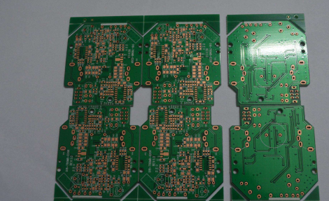
A Printed Circuit Board (PCB) is a flat board made of insulating material, typically fiberglass, with conductive pathways etched or printed onto its surface. These pathways, known as traces, connect various electronic components such as resistors, capacitors, integrated circuits (ICs), and connectors, allowing them to communicate and function together as a complete electronic circuit.
1.2. Types of PCBs
PCBs come in various types, each suited for different applications:
- Single-Sided PCBs: These have conductive traces on only one side of the board. They are simple and cost-effective, used in basic electronic devices.
- Double-Sided PCBs: These have conductive traces on both sides, allowing for more complex circuits. They are commonly used in consumer electronics.
- Multilayer PCBs: These consist of multiple layers of conductive traces separated by insulating layers. They are used in high-density and high-performance applications such as smartphones and computers.
- Flexible PCBs: Made from flexible materials, these PCBs can bend and twist, making them ideal for wearable electronics and compact devices.
- Rigid-Flex PCBs: Combining rigid and flexible sections, these PCBs offer the benefits of both types, used in aerospace and medical devices.
2. PCB Design and Manufacturing
2.1. PCB Design Process
The design of a PCB is a critical step that determines its functionality and performance:
- Schematic Design: The first step involves creating a schematic diagram that represents the electrical connections between components.
- Component Placement: Components are placed on the PCB layout, considering factors such as signal integrity, thermal management, and manufacturability.
- Routing: Traces are routed to connect the components according to the schematic. This step requires careful planning to avoid signal interference and ensure efficient heat dissipation.
- Design Rule Check (DRC): The design is checked against a set of rules to ensure it meets manufacturing and performance criteria.
- Gerber Files: The final design is exported as Gerber files, which are used by manufacturers to produce the PCB.
2.2. PCB Manufacturing Process
The manufacturing of PCBs involves several precise steps:
- Substrate Preparation: The base material, typically fiberglass, is prepared and cleaned.
- Copper Cladding: A thin layer of copper is laminated onto the substrate.
- Photoresist Application: A photoresist layer is applied to the copper-clad substrate.
- Exposure and Development: The photoresist is exposed to UV light through a mask, and the unexposed areas are developed away, leaving a pattern of traces.
- Etching: The exposed copper is etched away, leaving only the desired traces.
- Drilling: Holes are drilled for through-hole components and vias.
- Plating: The holes are plated with copper to create electrical connections between layers.
- Solder Mask Application: A solder mask is applied to protect the traces and prevent solder bridges.
- Silkscreen Printing: Component labels and identifiers are printed on the board.
- Testing and Inspection: The finished PCB is tested for functionality and inspected for defects.
3. Applications of PCBs
3.1. Consumer Electronics
PCBs are ubiquitous in consumer electronics, including:
- Smartphones and Tablets: High-density multilayer PCBs are used to accommodate the complex circuitry of modern mobile devices.
- Computers and Laptops: PCBs in these devices support processors, memory, and other critical components.
- Home Appliances: From microwaves to washing machines, PCBs control the functionality of various household devices.
3.2. Industrial Electronics
In industrial settings, PCBs are used in:
- Control Systems: PCBs are integral to the operation of industrial control systems, including PLCs (Programmable Logic Controllers) and SCADA (Supervisory Control and Data Acquisition) systems.
- Power Supplies: PCBs in power supplies manage the conversion and regulation of electrical power.
- Automation Equipment: PCBs enable the automation of manufacturing processes, improving efficiency and precision.
3.3. Automotive Electronics
The automotive industry relies heavily on PCBs for:
- Engine Control Units (ECUs): PCBs in ECUs manage engine performance, fuel injection, and emissions control.
- Infotainment Systems: PCBs support the functionality of in-car entertainment and navigation systems.
- Safety Systems: PCBs are used in airbag control modules, anti-lock braking systems (ABS), and advanced driver-assistance systems (ADAS).
3.4. Medical Devices
In the medical field, PCBs are critical for:
- Diagnostic Equipment: PCBs in devices such as MRI machines, CT scanners, and ultrasound equipment enable accurate diagnostics.
- Patient Monitoring: PCBs in wearable devices and hospital monitors track vital signs and provide real-time data.
- Therapeutic Devices: PCBs in devices such as pacemakers and infusion pumps deliver life-saving treatments.
3.5. Aerospace and Defense
PCBs in aerospace and defense applications must meet stringent reliability and performance standards:
- Avionics: PCBs in aircraft systems manage navigation, communication, and flight control.
- Satellites: PCBs in satellites support communication, data processing, and power management.
- Military Equipment: PCBs in military devices ensure reliable operation in harsh environments.
4. Latest Trends in PCB Technology
4.1. High-Density Interconnect (HDI) PCBs
HDI PCBs feature finer traces and smaller vias, allowing for higher component density and improved performance. They are used in compact devices such as smartphones and wearables.
4.2. Flexible and Rigid-Flex PCBs
The demand for flexible and rigid-flex PCBs is growing, driven by the need for compact and lightweight designs in wearable electronics, medical devices, and automotive applications.
4.3. Internet of Things (IoT)
The proliferation of IoT devices has increased the demand for PCBs that support wireless connectivity, low power consumption, and compact form factors.
4.4. Advanced Materials
New materials, such as high-frequency laminates and thermally conductive substrates, are being developed to meet the demands of high-performance applications.
4.5. Additive Manufacturing
Additive manufacturing, or 3D printing, is emerging as a potential method for producing PCBs, offering the possibility of rapid prototyping and customized designs.
5. Conclusion
PCBs are the cornerstone of modern electronics, enabling the functionality and performance of a wide range of devices across various industries. From design and manufacturing to applications and emerging trends, understanding the intricacies of PCB usage is essential for engineers, designers, and manufacturers. As technology continues to evolve, PCBs will play an increasingly critical role in shaping the future of electronics, driving innovation, and enabling new possibilities in the digital age.


