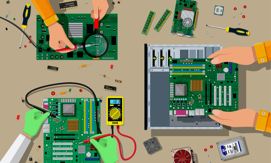
The Critical Importance of Component Placement in PCB Design
Introduction
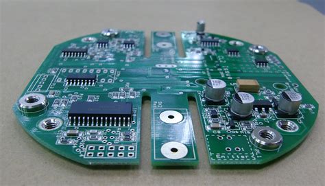
In the world of printed circuit board (PCB) design, component placement is often regarded as one of the most crucial stages in the entire design process. While novices might assume that routing connections between components is the primary challenge, experienced designers understand that proper component placement lays the foundation for a successful PCB. This article explores why component placement is so vital, examining its impact on functionality, manufacturability, signal integrity, thermal management, and overall product reliability.
The Foundation of PCB Functionality
Component placement serves as the architectural blueprint for how the entire circuit will function. Just as a poorly designed building layout leads to inefficient traffic flow and usability issues, improper component placement can create a cascade of problems throughout the PCB’s operation.
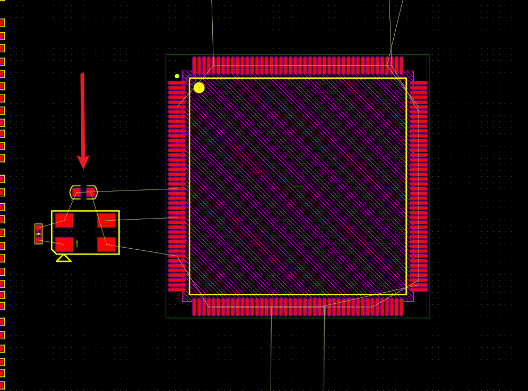
Circuit Performance Optimization: The physical arrangement of components directly affects electrical characteristics such as inductance, capacitance, and resistance in the circuit paths. Strategic placement minimizes parasitic effects that can degrade performance, especially in high-frequency applications. For instance, placing a decoupling capacitor too far from an IC’s power pin can render it ineffective at suppressing noise.
Signal Integrity Considerations: In modern electronics with high-speed signals, the time it takes for a signal to travel between components becomes critical. Proper placement ensures that timing requirements are met and that signal paths are of appropriate length. High-speed signals often require controlled impedance routing which is heavily dependent on proper component positioning.
Power Distribution Network (PDN) Design: Effective power delivery to all components begins with their placement. A well-planned component arrangement allows for an efficient power distribution network that minimizes voltage drops and ensures stable operation across the entire board.
Manufacturing and Assembly Implications
Component placement doesn’t just affect the board’s electrical performance—it significantly impacts how easily (or difficultly) the board can be manufactured and assembled.
Assembly Process Efficiency: Automated pick-and-place machines have specific requirements regarding component spacing and orientation. Proper placement considers these manufacturing constraints, reducing assembly time and cost. Components placed too close together may cause assembly difficulties, while those placed too far apart waste valuable board space.
Soldering Quality: The placement of components affects solder joint quality during reflow processes. Large thermal mass differences between nearby components can lead to tombstoning (where one end of a component lifts off the pad during soldering) or cold solder joints. Proper spacing and thermal balance are essential considerations.
Testability: Good placement facilitates easier testing and debugging. Test points should be accessible, and components should be arranged to allow probing without interference from adjacent parts. This becomes particularly important for boards that will undergo in-circuit testing (ICT) or flying probe testing.
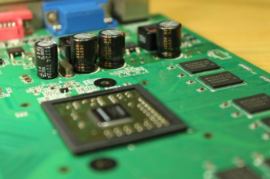
Thermal Management Through Placement
Heat generation and dissipation are critical factors in PCB reliability, and component placement plays a central role in thermal performance.
Heat Distribution: Placing all high-power components in one area can create hot spots that degrade performance and reduce component lifespan. Strategic spreading of heat-generating components across the board allows for better thermal distribution.
Natural Convection Considerations: For boards relying on natural air flow for cooling, component placement should facilitate rather than obstruct air movement. Tall components should generally be placed downstream of shorter ones to prevent creating thermal shadows.
Thermal Coupling: Some components are sensitive to temperature variations from nearby heat sources. Proper spacing or placement orientation can minimize unwanted thermal interactions between components.
Electromagnetic Compatibility (EMC) and Noise Reduction
Component placement is a powerful tool for addressing electromagnetic interference (EMI) issues, both as a source and victim.
Noise Source Isolation: Components that generate high-frequency noise (like switching regulators or clock generators) should be placed away from sensitive analog circuits. This physical separation reduces capacitive and inductive coupling of noise.
Current Loop Minimization: The placement of components affects current return paths. Keeping high-current loops small reduces their antenna effect and associated EMI radiation. This is particularly important for switching power supply layouts.
Shielding Considerations: Proper placement allows for effective use of shielding when needed, whether through physical shields or strategic grounding techniques. Components that require shielding should be placed in locations that facilitate this protection.
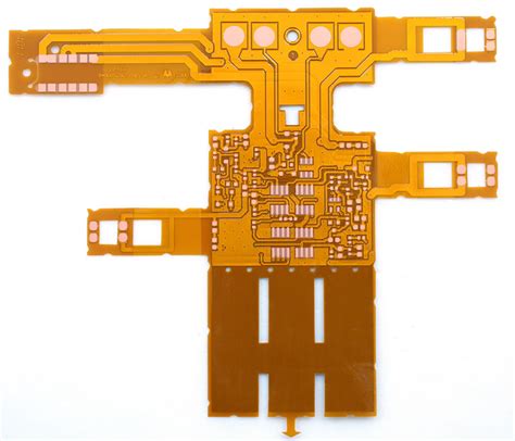
Density and Size Optimization
In today’s electronics, there’s constant pressure to reduce product size while increasing functionality—making efficient component placement essential.
Board Space Utilization: Careful placement maximizes the use of available board area, potentially reducing layer count or overall board size. This is especially critical for consumer electronics where miniaturization is a key competitive factor.
Layer Stack Planning: Good placement allows for more efficient routing, which can reduce the number of required layers in the PCB stackup—a significant cost factor in board fabrication.
Component Interaction: Some components may need to be placed on specific sides of the board due to mechanical constraints (like connectors) or thermal considerations (like heat sinks). Proper planning ensures all requirements are met without unnecessary compromises.
Design for Reliability and Serviceability
Component placement affects not just initial operation but long-term reliability and serviceability.
Mechanical Stress Considerations: Components should be placed to minimize stress on solder joints during operation or mechanical shock. This is particularly important for large or heavy components.
Service Access: In products that may require repair or maintenance, critical components should be placed in accessible locations. This includes fuses, adjustment potentiometers, or frequently replaced modules.
Vibration Resistance: Proper placement can improve a board’s resistance to vibration-induced failures. Strategic positioning and orientation of components can prevent resonant frequencies that might lead to fatigue failures.
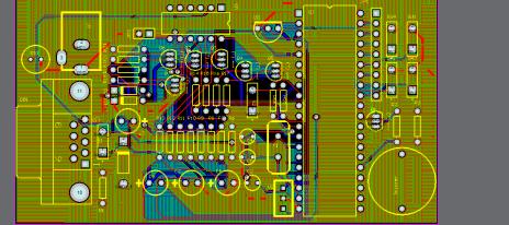
The Placement-Routing Interdependence
Component placement and trace routing are deeply interconnected aspects of PCB design.
Routing Complexity: Good placement naturally leads to simpler routing with fewer vias and crossovers. This improves signal integrity and reduces fabrication costs.
Differential Pair Routing: High-speed differential pairs require careful length matching that begins with proper component placement to allow for the necessary routing topology.
Bus Routing: Components connected by wide buses (like memory chips to processors) should be placed to allow for clean bus routing without excessive meandering or congestion.
Special Considerations for Different Technologies
Different types of electronics demand specific placement strategies.
Mixed-Signal Designs: These require careful partitioning of analog and digital sections with attention to grounding strategies that begin with component placement.
RF Circuits: RF designs need precise component placement to maintain controlled impedances and minimize stray reactances that could affect tuning and performance.
Power Electronics: High-voltage designs require adequate creepage and clearance distances that must be considered during placement.
The Human Factor in Placement
Even with advanced auto-placement tools, human expertise remains essential.
Design Intent Capture: Automated tools may optimize for one parameter (like wire length) while neglecting others (like thermal performance). Human oversight ensures all requirements are balanced.
Manufacturing Knowledge: Experienced designers incorporate knowledge of manufacturing capabilities and limitations that may not be captured in design rule checks.
Future Modifications: Anticipating potential design changes or variants can influence placement decisions to accommodate future needs.
Conclusion
Component placement in PCB design is far more than just an organizational step—it’s a critical process that influences nearly every aspect of a board’s performance, manufacturability, and reliability. While modern EDA tools offer increasingly sophisticated auto-placement capabilities, the strategic arrangement of components remains an area where engineering judgment and experience make a profound difference. From ensuring signal integrity to facilitating efficient manufacturing, from managing thermal issues to controlling EMI, proper component placement lays the groundwork for a successful PCB design. In an era where electronic products face ever-increasing demands for performance, reliability, and miniaturization, the importance of thoughtful component placement cannot be overstated. It truly is the foundation upon which all other aspects of PCB design are built.