The Evolution and Importance of Mobile Phone PCBs
Introduction to Mobile Phone PCBs
Printed Circuit Boards (PCBs) serve as the foundational framework for virtually all modern electronic devices, with mobile phones being one of the most prominent applications. The mobile phone PCB represents a marvel of modern engineering, packing increasingly complex circuitry into ever-shrinking form factors while maintaining reliability and performance. As smartphones have evolved from simple communication devices to powerful pocket computers, their PCBs have undergone remarkable transformations to accommodate new technologies, higher speeds, and more functionality.
The mobile phone PCB differs significantly from PCBs used in other electronic devices due to its unique requirements: extreme miniaturization, high-density interconnects, multi-layer construction, and stringent reliability standards. These specialized circuit boards must withstand mechanical stress, temperature fluctuations, and constant use while delivering flawless performance. This article explores the design considerations, manufacturing processes, materials, and technological advancements that make modern mobile phone PCBs possible.
Design Considerations for Mobile Phone PCBs
Miniaturization Challenges
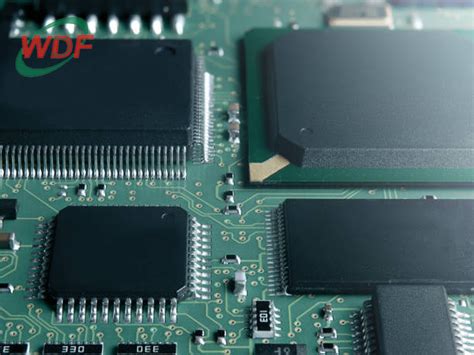
The relentless push for thinner, lighter smartphones has driven PCB technology to its limits. Modern mobile phone PCBs typically use High-Density Interconnect (HDI) technology, which allows for finer lines and spaces, smaller vias, and higher connection pad density. Designers must balance the need for compact layouts with thermal management concerns and signal integrity requirements.
Component placement becomes increasingly critical as board space shrinks. The proximity of high-speed digital circuits, RF components, and analog sections requires careful planning to prevent interference. Designers often use 3D modeling software to optimize component placement in the limited z-height available in slim smartphones.
Multi-layer Architecture
Contemporary smartphone PCBs commonly feature 8 to 12 layers, with some flagship models incorporating up to 16 layers. This multi-layer approach allows for better signal routing, improved power distribution, and enhanced EMI shielding. Typical layer stack-ups include:
- Signal layers for high-speed digital circuits
- Dedicated ground planes for noise reduction
- Power planes for stable voltage distribution
- Specialized layers for RF shielding
The arrangement of these layers follows strict design rules to maintain signal integrity, particularly for high-frequency components like 5G modems and WiFi chips.
Thermal Management
With powerful processors and fast-charging capabilities, thermal management has become a critical design factor. Mobile phone PCBs incorporate various techniques to dissipate heat:
- Thermal vias to transfer heat to other layers
- Copper pours in power sections
- Strategic placement of heat-generating components
- Thermal interface materials connecting to chassis or heat spreaders
Designers must carefully model thermal characteristics to prevent localized hot spots that could degrade performance or reduce component lifespan.
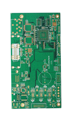
Materials and Manufacturing Processes
Advanced PCB Materials
The choice of substrate material significantly impacts the PCB’s performance, reliability, and cost. Common materials for mobile phone PCBs include:
- FR-4: The traditional epoxy-glass composite, often used in cost-sensitive designs or less demanding applications.
- High-Tg FR-4: Modified FR-4 with higher glass transition temperature for better thermal performance.
- Polyimide: Offers excellent thermal stability and flexibility, used in rigid-flex designs.
- Rogers Materials: High-frequency laminates for RF sections, providing stable dielectric properties.
- Halogen-free Materials: Environmentally friendly alternatives meeting RoHS requirements.
HDI Manufacturing Techniques
The production of mobile phone PCBs employs specialized HDI manufacturing processes:
- Laser Drilling: Creates microvias as small as 25-50μm in diameter, enabling high-density interconnects.
- Sequential Lamination: Builds up the board layer by layer for complex multi-layer structures.
- Fine Line Imaging: Achieves trace widths and spaces down to 30μm or less.
- Via-in-Pad: Places vias directly in component pads to save space.
- Any-layer HDI: Allows vias to connect any layers, maximizing routing flexibility.
Surface Finishes
The choice of surface finish affects solderability, durability, and signal integrity:
- ENIG (Electroless Nickel Immersion Gold): Common for high-reliability applications, excellent for fine-pitch components.
- OSP (Organic Solderability Preservative): Cost-effective but less durable.
- Immersion Silver: Good solderability and lower cost than ENIG.
- ENEPIG (Electroless Nickel Electroless Palladium Immersion Gold): Premium finish for challenging applications.
Key Components and Their PCB Integration
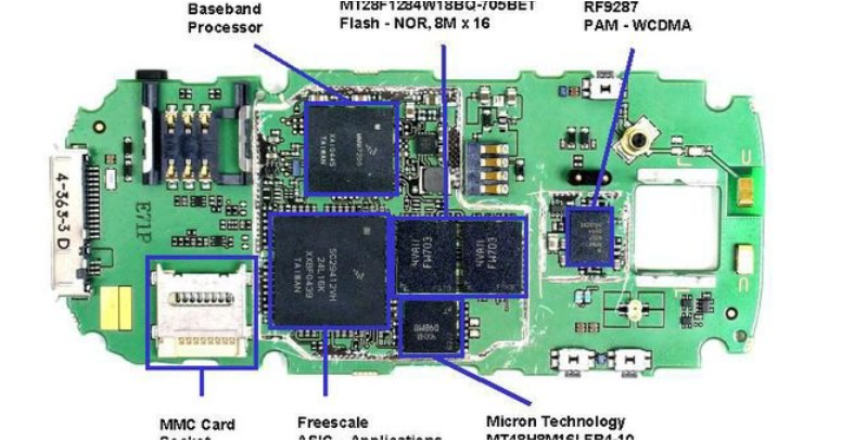
Application Processors and Memory
Modern System-on-Chip (SoC) processors and memory packages present significant PCB integration challenges:
- Package-on-Package (PoP): Stacks memory directly on top of the processor to save space.
- Fine-pitch BGAs: Ball Grid Array packages with pitch down to 0.3mm require precise PCB pad design.
- Embedded Components: Some passive components are buried within the PCB layers.
RF and Wireless Modules
The RF section demands careful PCB design:
- Antenna Integration: PCB traces often form part of the antenna system.
- Impedance Control: Critical for high-frequency signals (5G, WiFi 6, etc.).
- Shielding: Metal cans or conductive coatings prevent interference.
Power Management
Modern power delivery systems include:
- Distributed Power Architecture: Multiple voltage regulators placed near their loads.
- Battery Management: Charging circuits and fuel gauges integrated into the PCB.
- High-current Traces: Thick copper or embedded bus bars for power delivery.
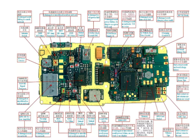
Reliability and Testing
Environmental Stress Testing
Mobile phone PCBs undergo rigorous testing:
- Thermal Cycling: Simulates temperature variations during use.
- Drop Testing: Evaluates mechanical robustness.
- Humidity Exposure: Assesses moisture resistance.
- Bend Testing: For flexible PCB sections.
Electrical Testing
Comprehensive electrical verification includes:
- Automated Optical Inspection (AOI): Checks for manufacturing defects.
- In-Circuit Testing (ICT): Verifies component functionality.
- Flying Probe Testing: For high-density boards where bed-of-nails fixtures aren’t feasible.
- Boundary Scan: Tests digital interconnections.
Future Trends in Mobile Phone PCB Technology
Embedded Components
The next frontier in miniaturization involves embedding active and passive components within the PCB layers, saving surface space and improving electrical performance.
Flexible and Rigid-Flex PCBs
Foldable phones have driven adoption of flexible PCBs, requiring new materials and design approaches that accommodate repeated bending.
Higher Frequency Materials
As 5G mmWave and future 6G technologies emerge, PCB materials must support even higher frequencies with low loss.
Additive Manufacturing
3D printing technologies may enable new PCB architectures with non-planar geometries and integrated features.
Advanced Thermal Management
With increasing power densities, innovative cooling solutions like vapor chambers or graphene layers may become integrated into PCB designs.
Conclusion
The mobile phone PCB represents one of the most sophisticated applications of printed circuit board technology, pushing the boundaries of miniaturization, performance, and reliability. As smartphones continue to incorporate more features and capabilities, PCB technology must evolve to meet these demands. From materials science to manufacturing processes, the innovations developed for mobile phone PCBs often find their way into other electronic devices, making this field a driver of progress for the entire electronics industry. The future will likely bring even more integration, flexibility, and performance as PCB technology keeps pace with the relentless advancement of mobile devices.