The Evolution and Importance of Printed Circuit Boards (PCBs) in Modern Computing
Introduction to PCBs
Printed Circuit Boards (PCBs) form the foundational infrastructure of virtually all modern electronic devices, serving as the central nervous system that connects and supports various electronic components. In the realm of computing, PCBs are particularly crucial, enabling the complex interconnection of processors, memory modules, power systems, and peripheral interfaces that make computers function.
A PCB is essentially a flat board made of insulating material (typically fiberglass) with conductive pathways—usually made of copper—etched or printed onto its surface. These pathways, known as traces, electrically connect different components mounted on the board without the need for messy and unreliable wire connections. The development of PCB technology has paralleled and enabled the exponential growth of computing power over the past several decades.
Historical Development of PCB Technology
The evolution of PCB technology reveals a fascinating journey of innovation that has transformed computing:
Early Beginnings (1920s-1940s):
The concept of printed wiring emerged in the early 20th century, with innovators like Charles Ducas filing patents for methods to create electrical paths directly on insulated surfaces. However, it wasn’t until World War II that PCB technology saw significant development, driven by military needs for reliable, compact electronics in equipment like proximity fuses.
Post-War Commercialization (1950s-1960s):
The 1950s saw the transition of PCB technology from military to commercial applications. Early computers like the IBM 650 used primitive versions of PCBs. The invention of the through-hole technology (THT) method, where component leads are inserted into drilled holes and soldered to pads on the opposite side, became standard practice.
The Integrated Circuit Revolution (1970s-1980s):
The advent of integrated circuits (ICs) created new demands for PCB technology. As chips became more complex with higher pin counts, the single-sided boards of the past gave way to double-sided and then multi-layer boards. The surface-mount technology (SMT) emerged during this period, allowing components to be mounted directly onto the surface of PCBs without requiring drilled holes.
Modern Era (1990s-Present):
Contemporary PCB design has become incredibly sophisticated, with high-density interconnect (HDI) technology allowing for finer traces and spaces, blind and buried vias for complex multi-layer routing, and advanced materials for high-speed and high-frequency applications. Modern computer motherboards may contain up to 12 or more layers of copper traces sandwiched between insulating material.
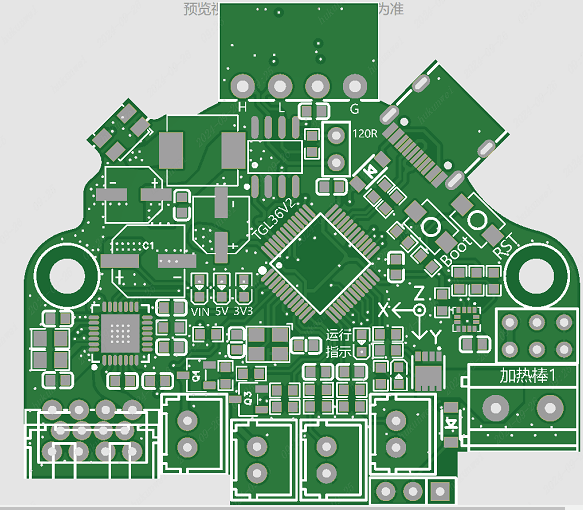
Anatomy of a Computer PCB
Understanding the physical composition of a typical computer PCB helps appreciate its complexity:
Substrate Material:
The base of a PCB is typically made from FR-4, a flame-retardant fiberglass-epoxy composite. High-performance computing applications might use more advanced materials like polyimide or ceramic-filled hydrocarbons for better thermal and electrical properties.
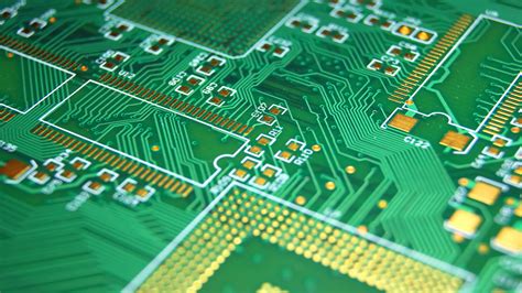
Conductive Layers:
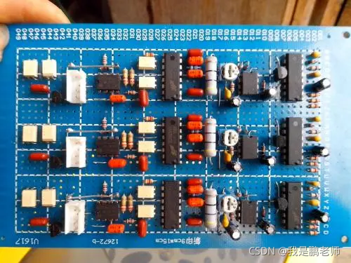
Copper foil is laminated onto the substrate and then etched to form the circuit patterns. Simple boards might have just one or two layers, while complex computer motherboards can have 8-12 layers or more, with intricate interconnections between them.
Solder Mask:
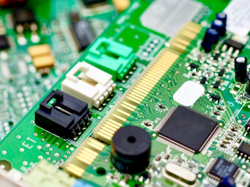
This polymer coating covers the copper traces to prevent oxidation and accidental short circuits, typically appearing green (though other colors are possible). It leaves only the component pads exposed for soldering.
Silkscreen:
The white (or other color) markings on a PCB that indicate component placement, orientation, and other identifying information. These are purely for human reference and don’t affect functionality.
Vias:
These are plated-through holes that allow connections between different layers of the PCB. They can be through-hole (going all the way through the board), blind (connecting an outer layer to one or more inner layers), or buried (connecting only inner layers).
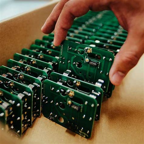
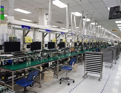
PCB Manufacturing Process
The creation of a computer PCB is a multi-stage process requiring precision and quality control:
- Design and Layout:
Using specialized Electronic Design Automation (EDA) software, engineers create schematic diagrams that are then translated into physical board layouts, considering factors like signal integrity, power distribution, and thermal management. - Printing the Design:
The layout is printed onto films that will be used to create the actual boards. For multi-layer boards, this is done for each layer separately. - Substrate Preparation:
The base material is cleaned and prepared for copper lamination. - Copper Lamination and Patterning:
Copper foil is laminated onto the substrate, and the circuit pattern is transferred using photolithography or direct imaging techniques. - Etching:
Chemical solutions remove unwanted copper, leaving only the desired circuit traces. - Layer Alignment and Lamination:
For multi-layer boards, the individual layers are carefully aligned and bonded together under heat and pressure. - Drilling:
Holes are drilled for through-hole components and vias. High-precision CNC machines ensure accuracy. - Plating:
The holes are plated with copper to establish electrical connections between layers. - Solder Mask Application:
The protective solder mask is applied and cured. - Surface Finishing:
Exposed copper areas receive a surface finish (like HASL, ENIG, or immersion silver) to prevent oxidation and ensure good solderability. - Silkscreen Printing:
Component identifiers and other markings are added. - Testing:
Electrical tests verify all connections are correct, and automated optical inspection (AOI) checks for physical defects.
Types of PCBs in Computing
Different computing applications require different PCB configurations:
Single-Sided PCBs:
The simplest type, with components on one side and conductive traces on the other. Rare in modern computing except for very simple peripheral devices.
Double-Sided PCBs:
Traces on both sides, with connections made through vias. Common in simpler computing devices or peripheral cards.
Multi-Layer PCBs:
Standard in modern computers, with 4-12 or more layers of traces sandwiched together. Allows for complex routing needed by modern processors and chipsets.
Rigid PCBs:
The most common type in desktop computers and servers, made from solid, inflexible material.
Flexible PCBs:
Made from flexible plastic materials, used in laptops for connections between moving parts or in wearable computers.
Rigid-Flex PCBs:
Combine rigid and flexible sections, useful in space-constrained applications like laptop motherboards where components need to fit in three dimensions.
PCB Design Considerations for Computers
Designing a PCB for computing applications involves numerous technical considerations:
Signal Integrity:
At high speeds (modern processors operate in the GHz range), traces act as transmission lines. Careful control of impedance, crosstalk, and signal reflections is crucial.
Power Distribution:
Modern CPUs can draw over 100 amps at low voltages. The power delivery network must provide clean, stable power with minimal voltage drop.
Thermal Management:
High-performance components generate significant heat. PCB design must incorporate proper thermal vias, copper pours, and sometimes embedded heat pipes or other cooling solutions.
Electromagnetic Compatibility (EMC):
Proper shielding and grounding are necessary to prevent interference with other devices and ensure the computer meets regulatory standards.
Component Density:
Modern computer PCBs pack an incredible number of components into small spaces, requiring careful placement and routing strategies.
Manufacturability:
Designs must balance performance with practical manufacturing constraints and costs.
Advanced PCB Technologies in Modern Computing
Recent advancements in PCB technology continue to push the boundaries of computer performance:
High-Density Interconnect (HDI):
Allows for finer traces and spaces (under 100 microns), smaller vias, and higher connection pad density. Essential for modern processors and chipsets.
Embedded Components:
Passive components like resistors and capacitors can be embedded within the PCB layers, saving space and improving performance.
Advanced Materials:
Low-loss dielectrics for high-speed signals, materials with better thermal conductivity, and substrates with carefully controlled dielectric constants.
3D Printing of PCBs:
Emerging additive manufacturing techniques may revolutionize prototyping and small-scale production.
Optical Interconnects:
Experimental PCBs that use both electrical and optical pathways for extremely high-bandwidth communication between components.
The Future of PCBs in Computing
As computing continues to evolve, PCB technology must adapt to new challenges:
Quantum Computing:
Will require PCBs capable of operating at cryogenic temperatures with minimal signal loss.
AI Accelerators:
The unique architectures of AI/ML processors demand innovative PCB approaches to handle massive parallel processing.
IoT Edge Devices:
Push for smaller, lower-power PCBs with integrated wireless capabilities.
Sustainable Computing:
Development of more environmentally friendly PCB materials and manufacturing processes.
Conclusion
From the simple single-layer boards of early computers to the incredibly complex multi-layer HDI designs in modern systems, PCBs have been the unsung heroes of the computing revolution. As the physical platform that brings silicon to life, PCB technology continues to evolve to meet the ever-increasing demands of processor speed, power efficiency, and miniaturization. Understanding PCB design and manufacturing is essential for anyone involved in computer engineering, as these unassuming boards will undoubtedly remain at the heart of computing innovation for decades to come.
The next time you use a computer—whether a smartphone, laptop, or data center server—take a moment to appreciate the intricate network of copper and fiberglass that makes it all possible. The humble PCB is truly one of the most important and underappreciated technologies of the digital age.